
Wafer-Dedicated SIMS: IMS Wf & SC Ultra
The CAMECA IMS Wf and SC Ultra are magnetic sector Secondary Ion Mass Spectrometers dedicated to advanced semiconductor process control and ultra-shallow depth profiling.
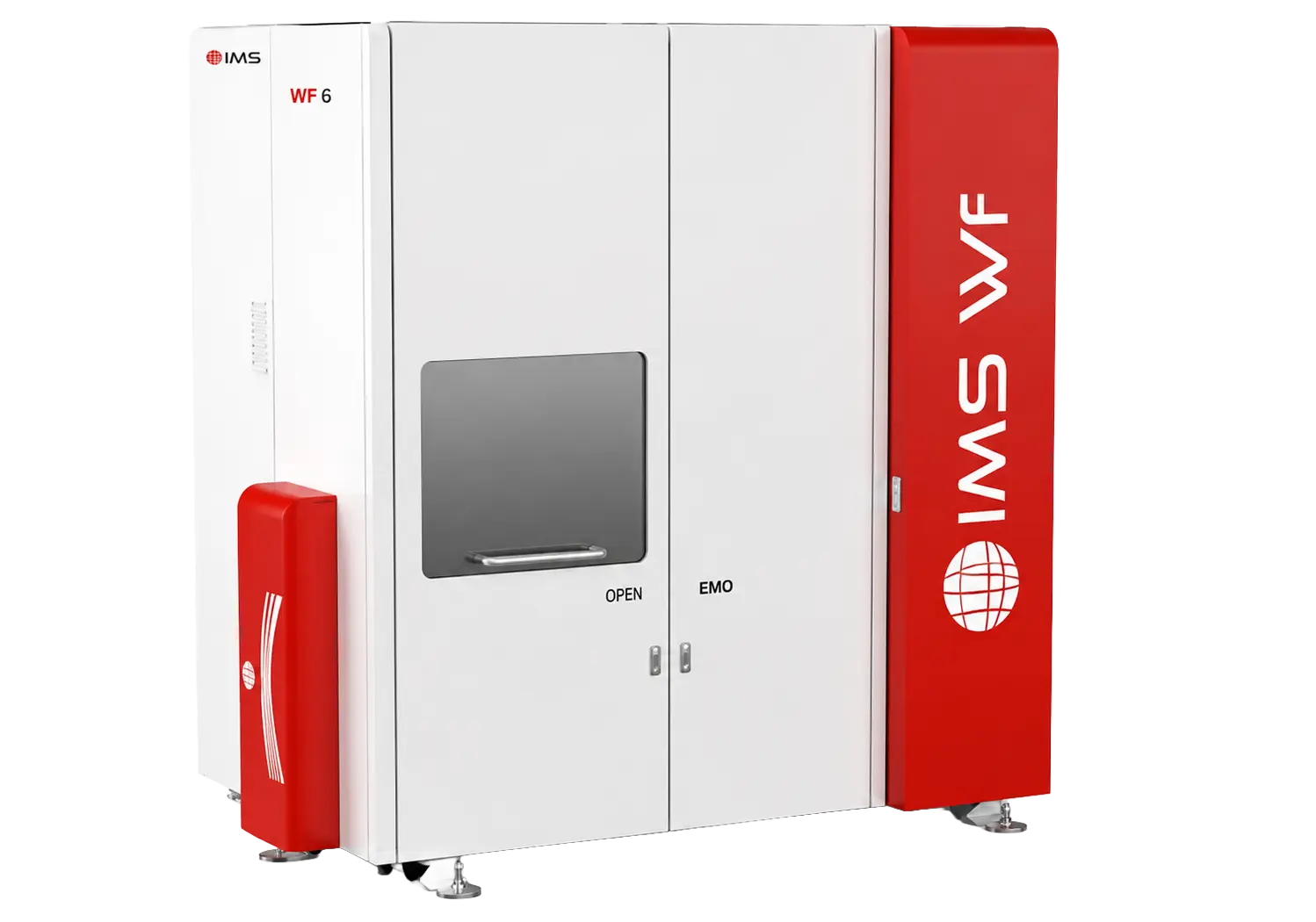
Manufacturer: CAMECA — France
Overview
The CAMECA IMS Wf and SC Ultra are magnetic sector Secondary Ion Mass Spectrometers dedicated to advanced semiconductor process control and ultra-shallow depth profiling. They are the only SIMS instruments offering EXtreme Low Impact Energy (EXLIE) capability, sputtering across a wide range of impact energies from 150 eV to 13 keV without compromising mass resolution, primary beam density, or analytical throughput. The IMS Wf is configured for full 300 mm wafer handling and high-volume automated analysis, while the SC Ultra accommodates a 75 mm × 75 mm sample holder for laboratory-scale characterization work. Both instruments deliver depth resolution better than 1 nm per decade, making them the tool of choice for extra-shallow implants, high-k metal gates, SiGe doped layers, Si:C:P structures, oxynitrides, PV and LED devices, and graphene. Their high level of automation, combined with the SmartPro/WinCurve software suite, ensures reproducible, unattended, high-throughput operation for fab-level process qualification.
Measurement Principle
The IMS Wf and SC Ultra are dynamic SIMS instruments based on CAMECA's magnetic sector, double-focusing mass spectrometer design with fast peak-switching capability. Two primary columns can be mounted simultaneously: a 60° floating column with a cesium ion source and impact energies from 150 eV to 13 keV, and a 36° standard column with an RF-plasma oxygen source running in acceleration-deceleration mode from 100 eV to 10 keV. This flexible primary column configuration lets operators select the ideal sputtering species, angle, and energy for each application without compromising mass resolution or beam density.
Depth Profiling Performance & Depth Resolution
By operating at Ultra-Low Impact Energies down to 150 eV, the IMS Wf and SC Ultra achieve sub-nanometer depth resolution while preserving accurate near-surface quantification of implanted dopant species. Depth profile accuracy has been validated against quantitative NRA, RBS, HR-RBS, and ERDA reference techniques. A dedicated MESA sample preparation mode eliminates crater edge effects during small-area analysis, further improving dynamic range on test patterns as small as 100 × 100 µm².
Automation & Wafer Handling / Throughput
The IMS Wf's airlock system, sample stage, and analysis chamber accommodate wafers up to 300 mm, with a robotic storage chamber and fully motorized transfer that can chain up to 100 samples in unattended, automated sequences. The SC Ultra instead uses a 75 mm × 75 mm sample holder with multiple window configurations that can carry up to 25 samples, with manual holder transfer suited to flexible laboratory use. Both models support remote monitoring from a distant PC so multiple users can launch sequences and review acquired data without being physically present at the tool.
Primary Ion Sources
The 60° floating column is equipped with a cesium ion source optimized for high primary beam density at very low impact energies, while the 36° standard column carries a high-brightness RF-plasma oxygen source. Both sources deliver sputter rates of several nm/min even at 150 eV for Cs and O2 alike, enabling high-throughput profiling at sub-nanometer depth resolution. An optional low-energy cesium ion source upgrade further extends Extremely Low Impact Depth Profiling capability for nanometer-scale layers.
Detection & Mass Spectrometer
Secondary ions are detected using a combination of one Faraday Cup and one Electron Multiplier, providing a counting system with a dynamic range of 10 decades. A Normal-Incidence Electron Gun (NEG) supplies low-energy electrons with auto-compensation of charging effects, ensuring reproducible analysis on insulating materials. High mass resolving power, up to MRP = 10,000, resolves close mass interferences such as 75As- from 74GeH and 30Si29Si16O in SiGe layers.
Applications
The IMS Wf and SC Ultra address deep-to-ultra-shallow implant monitoring, HKMG and SiON thin film metrology, SiGe and Si:C:P doped-layer characterization, and optoelectronic and LED device development, including impurity control of O, H, and C at the lowest detection limits on the market. Full 300 mm wafer mapping with sub-percent precision supports implanter and thin-film growth tool qualification directly in production environments. An optional fully eucentric rotation stage reduces the impact of surface roughness on depth resolution during metal thin film analysis.
Software
The SmartPro WinCurve software suite provides a database-centered workflow covering tool calibration, data acquisition, analytical recipe selection, and chain batch processing for fully automated analysis. Checkerboard acquisition and post-processing lets operators optimize the crater gate after measurement to reject edge effects and dust artifacts without re-running the analysis. WinImage adds powerful image visualization, 3D reconstruction, and batch processing capabilities built on the Aphelion imaging libraries.
Common Specifications
| Specification | IMS Wf & SC Ultra |
|---|---|
| Primary ion sources | Cs⁺ (60° floating column), O2⁺ RF-plasma (36° standard column) |
| Impact energy range – 60° Cs column | 150 eV to 13 keV |
| Impact energy range – 36° O2/RF-plasma column | 100 eV to 10 keV |
| Depth resolution | < 1 nm/decade |
| Mass resolving power | Up to MRP = 10,000 |
| Detection system | Faraday Cup + Electron Multiplier, 10 decades dynamic range |
| Electron gun | Normal-Incidence Electron Gun (NEG) for charge compensation |
| Mass spectrometer | Magnetic sector, double focusing, fast peak switching |
| Analytical chamber vacuum | 10⁻¹⁰ mbar range |
| Full wafer mapping | Up to 300 mm wafers, 25-point mapping |
| Repeatability | Sub-percent precision (dose variation σ = 0.3%) |
| Oxygen flooding | Standard |
| S2/S8 certification | Standard |
Configuration Comparison
| Specification | IMS Wf | SC Ultra |
|---|---|---|
| Sample stage | XYZ axes, 300 mm stage | XYZ axes, 75 mm stage |
| Maximum wafer/sample size | Up to 300 mm wafers | 75 mm × 75 mm sample holder (multiple window configurations) |
| Sample capacity per batch | Up to 100 samples (multiple shuttles) | Up to 25 samples |
| Sample transfer | Fully automated transfer robot | Manual sample holder transfer |
| 60° floating column (Cs source) | Included | Included |
| RF-Plasma ion source (36° column) | Included | Included |
| Motorized diaphragms and slits | Included | Included |
| Oxygen flooding | Included | Included |
| S2/S8 certification | Included | Included |