
Inline Wafer SIMS: AKONIS
The CAMECA AKONIS is a fully automated inline Secondary Ion Mass Spectrometer engineered for high-volume semiconductor manufacturing environments where fab-level process control and tool-to-tool matching are required.
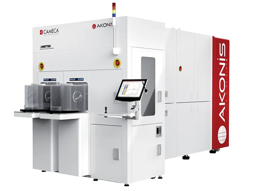
Manufacturer: CAMECA — France
Overview
The CAMECA AKONIS is a fully automated inline Secondary Ion Mass Spectrometer engineered for high-volume semiconductor manufacturing environments where fab-level process control and tool-to-tool matching are required. It performs on-the-fly composition measurements, delivering high-precision implant profiles, compositional analysis, and interfacial data directly within the fab rather than in an off-line characterization lab. AKONIS is built around a new EXtremely Low Impact Energy (EXLIE) ionic column operating below 150 eV, paired with a full wafer handling system and a high-resolution interferometric stage capable of measuring pads as small as 20 µm. Complementing CAMECA's IMS Wf/SC Ultra and SIMS 4550 platforms used in characterization labs, AKONIS extends SIMS excellence to the production floor with SEMI-certified automation and minimal operator expertise required. It is purpose-built to support demanding SiGe and SiP multilayer stack monitoring for N5 and beyond CMOS processes.
Measurement Principle
AKONIS is a dynamic Secondary Ion Mass Spectrometer that sputters a wafer surface with a primary ion beam and analyzes the ejected secondary ions to reveal composition and dopant depth distributions. Its high-density EXLIE column keeps spot size compatible with raster scans of less than 30 µm even at extremely low impact energies. Fully automatic primary column tuning and auto-adaptive secondary optics ensure the highest ionic collection efficiency on every measurement without operator intervention.
Depth Profiling Performance & Depth Resolution
The instrument achieves a depth resolution better than 1 nm per decade with a dynamic range of up to 5 decades, enabling accurate quantification of fast dopant profiles in SiGe and SiP multilayer stacks. Reproducibility and repeatability are both held to less than 1%, giving fabs the statistical confidence needed for tool-to-tool matching and statistical process control. The EXLIE column sustains a sputtering rate above 5 nm/min at 150 eV, five times higher than the previous generation, so high throughput is maintained even on thick stacks.
Automation & Wafer Handling / Throughput
AKONIS combines Brooks front-end wafer handling, a Pfeiffer vacuum-based system, and a Cognex-based pattern recognition engine to deliver full-wafer, blanket, and patterned measurements with minimal operator input. A high-resolution interferometric stage provides position accuracy better than 2 µm, allowing reliable measurement on test pads as small as 20 µm. The tool processes 8 wafers per hour with a pre-loadlock transfer of less than 90 seconds from airlock to analysis chamber, and it is rated for 95% uptime.
Primary Ion Source
AKONIS is built around a new high-density EXLIE (EXtremely Low Impact Energy) primary ion column operating below 150 eV. This column offers high RSF stability over time, automated beam alignment, and access to sub-nanometer depth resolution without sacrificing beam density or throughput. Low maintenance requirements for the primary ion source help reduce the total cost of ownership.
Detection
Fixed detectors with automatic beam centering ensure consistent secondary ion collection across long, unattended measurement campaigns. A new near-UV Optical Charge Compensation (OCE) technology enables reliable charging-effect compensation for insulator analysis. Automatic data output with selectable formats is fed directly into CAMECA's data treatment engines for immediate feedback to the process line.
Applications
AKONIS targets the most demanding semiconductor process control applications, including high-resolution composition and fast dopant depth profiling of SiGe and SiP multilayer stacks used in advanced CMOS transistors. It supports statistical process control of p-MOS logic through boron-in-SiGe monitoring and n-MOS logic through phosphorus and arsenic shallow implant metrology. The tool is SEMI certified (S2/S8, E4, E5, E39, E84) for direct integration into fab automation and data infrastructure.
Software
AKONIS uses an intuitive graphical user interface built around a unique material database, allowing fab operators without SIMS expertise to create analysis recipes quickly. Automated instrument set-up and acquisition routines reduce time to feedback data to the process line by more than 97% compared with conventional characterization workflows. The software supports 3D imaging reconstruction and high mass resolution analysis without compromising beam size or sensitivity.
Common Specifications
| Specification | AKONIS |
|---|---|
| Detection limit | ≤ 1×10¹⁴ atoms/cm³ |
| Depth resolution | < 1 nm/decade |
| Dynamic range | Up to 5 decades |
| Reproducibility | < 1% |
| Repeatability | < 1% |
| Minimum pad size | 20 µm |
| Throughput | 8 wafers per hour |
| Uptime | 95% |
| Primary column impact energy (EXLIE) | < 150 eV |
| Sputtering rate | > 5 nm/min @ 150 eV |
| Beam spot size | < 30 µm (raster scan compatible) |
| Position accuracy | < 2 µm |
| Airlock-to-analysis transfer time | < 90 seconds |
| SEMI certifications | S2/S8, E4, E5, E39, E84 |