
Field Emission Auger Microprobe: JAMP-9510F
The JAMP-9510F is a high-specification field emission Auger microprobe pairing a Schottky field emission gun with a hemispherical analyzer for high-throughput chemical-state analysis in nano to micro areas, with 3 nm SEM resolution and an 8 nm Auger probe.
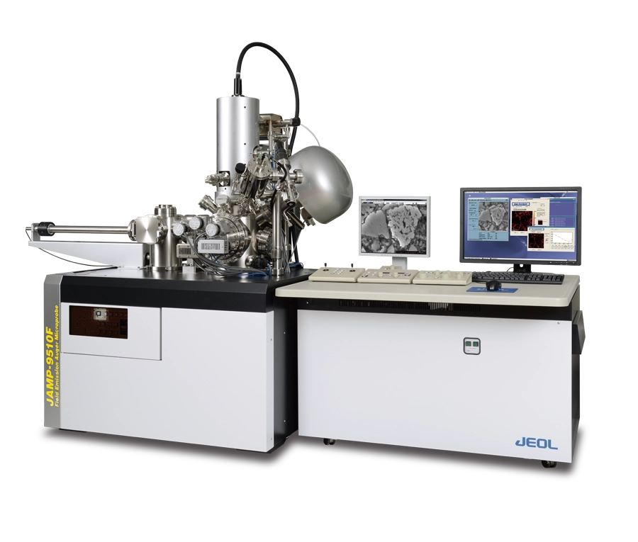
Manufacturer: JEOL — Japan
Overview
The JAMP-9510F is a high-specification field emission Auger microprobe combining a Schottky field emission electron gun — also used in JEOL's EPMA instruments for its large, stable probe current — with a hemispherical analyzer (HSA) for high-throughput analysis of chemical bonding states in nano to micro areas. An advanced electron optics system delivers stable SEM performance with 3 nm resolution, while a probe diameter of only 8 nm guarantees fine Auger analysis. Together with a highly precise eucentric specimen stage and a floating-type ion gun, the instrument handles any specimen — from metals to insulators — to obtain both compositional and chemical information.
High-Sensitivity Hemispherical Analyzer with Selectable Resolution
The latest HSA system allows the energy resolution to be adjusted between 0.05% and 0.6% to suit each element, improving map sensitivity up to five times over conventional Auger systems. The high-sensitivity mode acquires trace-element maps with a high signal-to-noise ratio — resolving, for example, the small carbon peak of cementite within a pearlite grain. The high-energy-resolution mode detects small peak shifts caused by chemical state differences, such as the chemical shift of nitrogen between BN and TiN in a cross-section of a cutting tool.
Spectrum Imaging
A newly developed spectrum imaging method captures an electron spectrum for each pixel in the image. Spectra from selected areas and elemental distributions can be extracted after acquisition, like EDS mapping. Because data are acquired over a wide energy range, no element is missed — a fundamental difference from conventional Auger mapping, where elements must be specified in advance. The measuring energy range and energy resolution are freely selectable, and spectrum imaging can be applied not only to elemental analysis but also to reflection electron energy loss spectroscopy (REELS).
Chemical State Analysis with Standard Spectra Database
Chemical state analysis in a nano-area delivers results comparable to XPS. Information about chemical state is contained in Auger peak shifts and shape changes, which the Spectra Investigator peak deconvolution software resolves in one click — without complicated parameter setting — by comparison against JEOL's original library of more than 500 standard spectra covering 140 materials. In depth profiling of lithium-ion battery cathode materials, this deconvolution reveals, for example, lithium enrichment inside particles where Mn²⁺ dominates over Mn⁴⁺.
Non-Conductive Material Analysis
Two key technologies enable Auger analysis of non-conductive materials in minute areas: a neutralization ion gun that irradiates Ar ions of only a few eV at high current, and an eucentric mechanical stage with a tilt angle of 0° to 90°. Together they make charge-free analysis possible on samples such as glass, ceramics, flexible polyimide circuit boards, and PTFE.
Applications
Semiconductor devices: with spatial resolution far beyond SEM-EDS or EPMA, AES resolves elemental and silicon chemical-state maps of device cross-sections at high magnification.
Lithium-ion battery materials: AES detects lithium in oxides and carbonates with high sensitivity, and lithium mapping is performed easily with spectrum imaging.
REELS analysis: reflection electron energy loss spectroscopy characterizes carbon materials — distinguishing graphite from amorphous carbon — and evaluates the bandgap of wide-bandgap semiconductors and insulators.
Expandability
Additional ports accommodate a range of attachments supporting a variety of analyses: a backscattered electron detector (BED), a specimen cooling and fracturing device, a specimen parking unit, a transfer vessel, electron backscatter diffraction (EBSD), and an energy dispersive X-ray spectrometer (EDS).
Specifications for JAMP-9510F Field Emission Auger Microprobe
| Specification | JAMP-9510F |
|---|---|
| Electron Gun | Schottky field emission gun |
| SEI Resolution | 3 nm (at 25 kV, 10 pA) |
| Probe Diameter for Auger Analysis | 8 nm (at 25 kV, 1 nA) |
| Accelerating Voltage | 0.5 kV to 30 kV |
| Probe Current | 10⁻¹¹ A to 2×10⁻⁷ A |
| Magnification | ×25 to ×500,000 |
| Analyzer | Electrostatic hemispherical analyzer (HSA) |
| Energy Resolution (ΔE/E) | 0.05% to 0.6% (selectable) |
| Sensitivity | 840,000 cps or more (7-channel detector; at 10 kV, 10 nA, Cu-LMM, 0.6% resolution, 60° tilt) |
| Specimen Stage Movement | X, Y: ±10 mm; Z: ±6 mm; tilt: 0° to 90°; rotation: 360° |
| Ion Gun Accelerating Voltage | 0.01 kV to 4 kV (10 V to 100 V for charge neutralization) |
| Analysis Chamber Ultimate Vacuum | 5×10⁻⁸ Pa or less |
| Power Supply | Single-phase 200 V AC, 50/60 Hz, 6 kVA; single-phase 100 V AC, 50/60 Hz, 3 kVA |
| Cooling Water | 0.08 MPa to 0.25 MPa (gauge pressure); flow rate 1.8 L/min to 2.2 L/min |
| Gas Supply | Compressed air 0.8 MPa to 1.0 MPa; dry nitrogen 0.4 MPa to 0.5 MPa; high-purity Ar gas 0.1 MPa to 0.2 MPa (purity 99.999% or better) |
| Installation Environment | Temperature 15 °C to 25 °C (fluctuation ±2 °C/h or less); humidity 20% to 60% (no condensation); magnetic field 0.2 µT (p-p) or less |
| Installation Space | Floor space 4,000 mm × 4,000 mm or more; entrance 1,000 mm (W) × 1,900 mm (H) |
| Total Instrument Weight | 1,560 kg |
| Principal Options | Backscattered electron detector (BED), specimen cooling and fracturing device, specimen parking unit, transfer vessel, electron backscatter diffraction (EBSD), energy dispersive X-ray spectrometer (EDS) |