
FE-SEM — Model: JSM-IT810
Versatility and high spatial resolution meet automation with the JSM-IT810 series FE-SEM. Built-in no-coding automation for imaging and EDS analysis streamlines the workflow, from high-throughput routine work to advanced materials research.
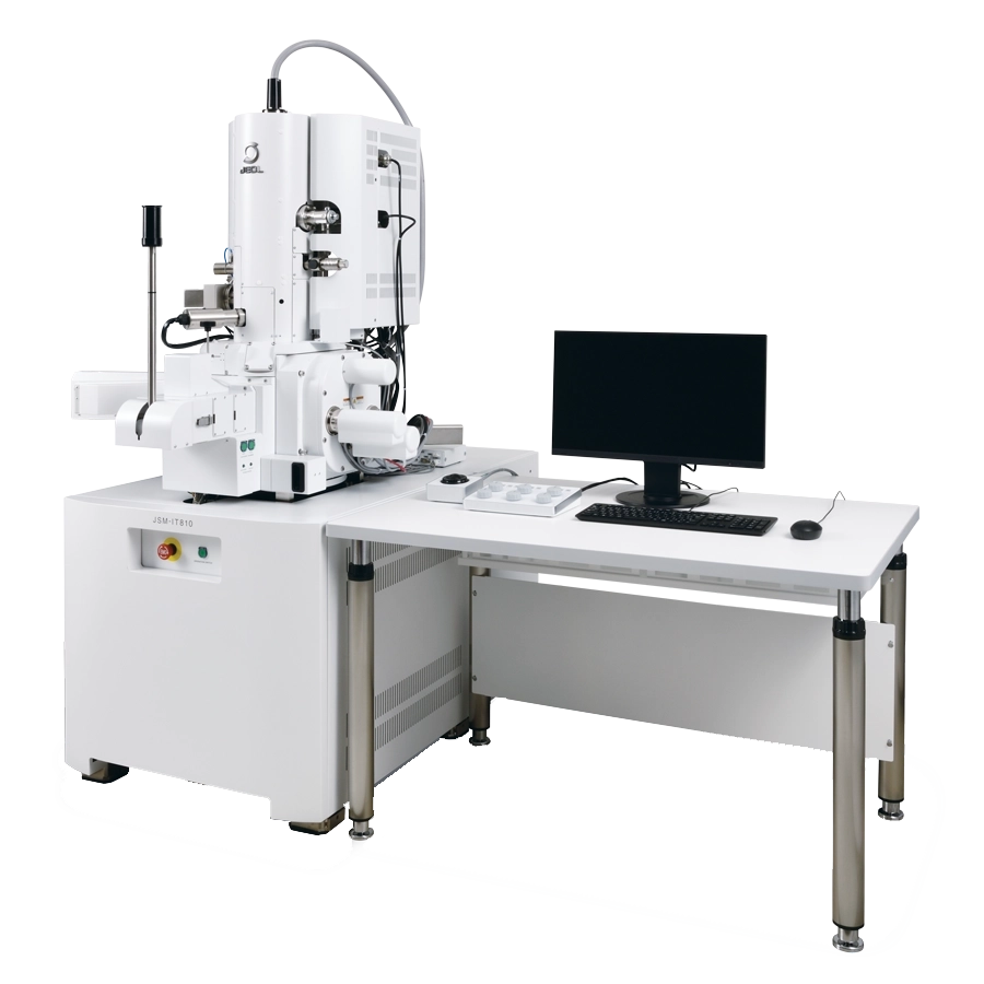
Manufacturer: JEOL — Japan
Overview
Versatility and high spatial resolution meet automation with the JSM-IT810 series FE-SEM.
No-coding automation for imaging and EDS analysis is built in for a streamlined and efficient workflow, and new functions ensure high-quality data and an enhanced user experience for all SEM users — including the SEM automatic adjustment package, a trapezoidal correction function (useful for EBSD measurements) and Live 3D surface reconstruction for observing surface topography.
Operating an FE-SEM has never been easier.
Features
Neo Action — A New Era in Automation
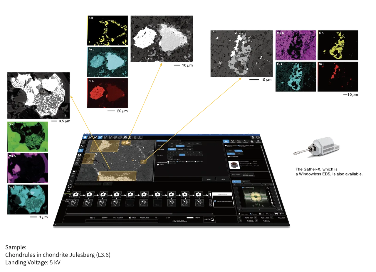
Neo Action provides no-code automation workflows, allowing even a novice user to effortlessly perform SEM observations and EDS analyses (requires a JEOL EDS detector). Areas of interest are selected, conditions registered, and the instrument executes the measurements automatically — demonstrated on chondrule-bearing meteorite sections with automated multi-point elemental mapping. The Gather-X windowless EDS is also available.
Link observation and elemental analysis — EDS integration
Live Analysis and Live Map (option) automatically provide the spectrum and elemental maps of the observation area in real time — effective for screening targets. Select point, area, map or line from the icons and click the target location on the live image to start analysis immediately. (Requires a JEOL EDS detector.).
Link optical and SEM images — Zeromag
Zeromag is built in for a seamless transition from optical to SEM imaging: as magnification changes, the image automatically switches between optical and SEM. Useful for locating the observation area and managing acquired data. (The optical stage navigation system SNS is required for optical images.).
Link data and reporting — SMILE VIEW™ Lab
Connectivity with SMILE VIEW™ Lab, JEOL's data management system: data is automatically saved per project and reports are created automatically from templates. With an additional license (option), analysis can be performed on PCs other than the instrument itself.
EDS Integration & Phase Analysis
The integrated design of EDS and SEM eliminates the barriers between observation and elemental analysis: point, area, mapping and line analyses are set up directly on the observation screen, and analysis starts with just three clicks — the interface switches to the analysis screen automatically.
The integrated EDS can automatically and quickly generate chemical-composition information corresponding to the elemental maps. On a metal-particle cross-section, phase analysis separated CoNi (63.07%), CrC (24.20%) and WCrC (12.74%) areas. (Optional function: Phase analysis).
In-lens Schottky Plus electron gun
Enhanced brightness through integration of the electron gun with the low-aberration condenser lens: probe currents from a few pA to several tens of nA even at low accelerating voltages, so high-resolution observation, high-speed elemental mapping, EBSD and SXES analysis are performed without objective-aperture switching. The emitter carries a three-year warranty.
Aperture angle Control Lens (ACL)
Positioned above the objective lens, the ACL automatically optimises the aperture angle across the entire current range — the smallest probe size is maintained even as probe current increases, from high-resolution observation to large-current analysis.
Beam deceleration (BD) mode
A bias voltage on the specimen stage decelerates the incident beam just before the specimen, improving spatial resolution and S/N at low landing voltage — available on all JSM-IT810s. SHL and SIL offer a higher biasing option on their PRIME versions for even higher resolution at lower voltages.
Three Versions: HL, SHL and SIL
The JSM-IT810 offers three objective-lens versions to match the task.
JSM-IT810(HL) — the basic model
The Hybrid Lens combines magnetic and electrostatic lenses for high-spatial-resolution imaging and analysis on all sample types, including magnetic materials and insulators.
JSM-IT810(SHL) — the multi-purpose model
The Super Hybrid Lens is an enhanced hybrid-lens design for even higher spatial resolution while keeping the hybrid lens's ease of use.
JSM-IT810(SIL) — the high-end model
The Semi-In-Lens forms a strong magnetic field below the objective lens for ultra-high spatial resolution.
Detectors to Match the Purpose
SBED — speed & sensitivity (option)
The scintillator backscattered electron detector enhances response and sensitivity over semiconductor types; combined with high-speed, high-resolution scanning, a wide area is captured quickly in high detail — a 10,240 × 7,680 pixel mouse-cerebellum image in 52 seconds at 0.64 µs/pixel.
VBED — signal selection & 3D (option)
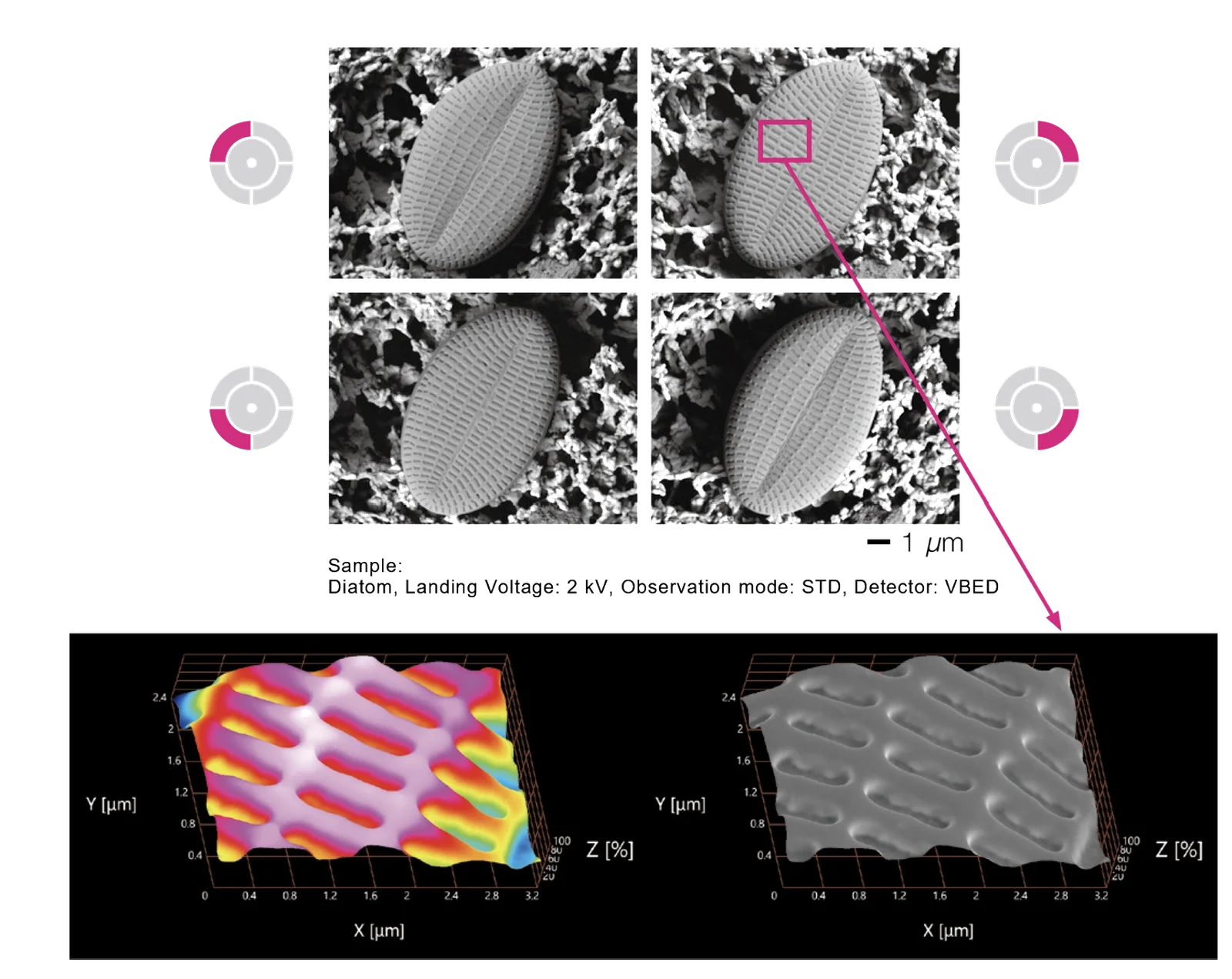
The versatile 5-segment semiconductor detector selectively collects backscattered signals; images from four directions allow 3D reconstruction of the specimen surface, and Live 3D displays a real-time 3D view for immediate assessment of topology.
A Variety of Functions for Multi-Purpose Measurement
Neo Engine — a next-generation electron-optical control system — delivers stable imaging quickly under any conditions and easier automatic operation.
Various automatic functions: advanced auto beam alignment (ABA) plus automatic focus, astigmatism and brightness.
Large Depth of Focus (LDF) mode: focusing via the ACL for low-distortion, large-area, deep-focus imaging of tall specimens.
Electron Channeling Pattern (ECP) mode (option) for crystalline specimens.
Low Vacuum (option): observation and analysis of insulating materials with no conductive coating (LVBED standard detector, 10 to 300 Pa, automatic orifice control).
Live-AI filter (option): machine-learning live-image enhancement with no residual image — very effective when searching for an observation area.
CAD Navigation (option): synchronises CAD position data with the SEM stage — effective for semiconductor specimens.
External control package (option): control the SEM and EDS from Python or C#, including automation and machine-learning integration.
SEM Automatic Adjustment package (option): three dedicated samples for magnification calibration, beam alignment and EDS energy calibration.
Abundant attachment ports
The multi-purpose chamber accepts a wide range of attachments — EDS, windowless Gather-X, SXES, EBSD, TED, multiple backscattered detectors, a hybrid specimen exchange chamber and stage options.
Specifications
| Specifications | JSM-IT810(HL) | JSM-IT810(SHL) | JSM-IT810(SIL) |
|---|---|---|---|
| Resolution | 0.7 nm | 0.6 nm | 0.6 nm |
| Magnification | ×10 to ×2,000,000 | ||
| Landing voltage | 0.01 to 30 kV | ||
| Electron gun | In-lens Schottky Plus field emission electron gun | ||
| Objective lens | Hybrid Lens (HL) | Super Hybrid Lens (SHL) | Semi-In-Lens (SIL) |
| Standard detectors | Secondary electron detector (SED) Upper electron detector (UED) Energy-dispersive X-ray spectrometer (EDS) | Secondary electron detector (SED) Upper hybrid detector (UHD) Energy-dispersive X-ray spectrometer (EDS) | Secondary electron detector (SED) Upper In-lens detector (UID) Energy-dispersive X-ray spectrometer (EDS) |
| Energy dispersive X-ray spectrometer (EDS) | SD detector with detection surface area: 60 mm² is included in the standard configuration. Resolution ≦ 129 eV for Mn Kα and Detectable Elements: Be to U | ||
| Automatic function | Beam alignment Focus / astigmatism / brightness / contrast correction | ||
| Major installable options | Backscattered electron detector (BED); Low-vacuum option - including low-vacuum backscattered electron detector (LVBED); Low-vacuum secondary electron detector (LVSED); Scintillator backscattered electron detector (SBED); Versatile backscattered electron detector (VBED); Energy dispersive X-ray spectrometer (EDS): SD detector with detection surface area: 30/60/100 mm²; Soft X-ray emission spectrometer (SXES); Wavelength dispersive X-Ray spectrometer (WDS); Electron backscatter diffraction system (EBSD); Transmission Electron Detector (TED); Specimen exchange chamber; Stage navigation system (SNS); Chamber camera; Operation panel; Track ball; SMILENAVI; SMILE VIEW™ Map |