
SEM — Model: JSM-IT710HR
The newly born JSM-IT710HR is the fourth-generation model of JEOL's HR series, which is based on the theme of "SEM that allows anyone to easily take high-resolution images".
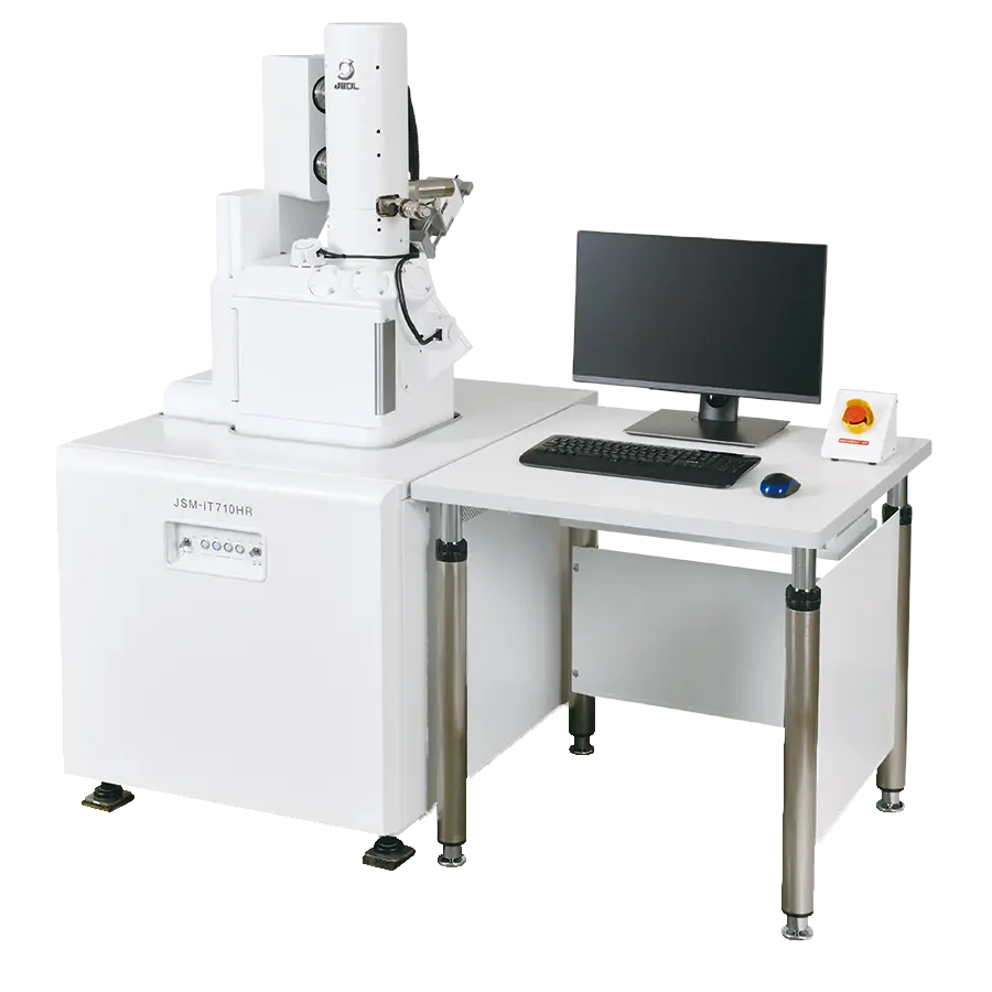
Manufacturer: JEOL — Japan
Overview
Today it is not only nanometre-order resolution and analytical performance that matter, but also throughput in data acquisition. The JSM-IT710HR is the fourth-generation model of JEOL's HR (High Resolution) series, built on the theme of an SEM that allows anyone to easily take high-resolution images.
With enhanced automatic functions for effortless operation and improved observation performance from a new detector, the JSM-IT710HR invites users to pursue what lies beyond what has already been seen.
Features
SEM and optical images, linked
The SEM image is visible in conjunction with the optical image, so navigation and observation flow naturally from the overview to the detail.
Seeing better with a high-resolution electron gun
The high-resolution electron gun sharpens the image itself — details emerge that previous-generation instruments left unseen.
Four ways to see more
Charge reduction under low vacuum for beam-sensitive specimens; 3D observation with the multi-segment detector; elemental information with EDS (optional); and crystal-structure analysis with EBSD (optional).
Automatic Observation: Simple SEM / EDS
The Simple SEM function enables automatic measurements by registering multiple conditions at once, improving the efficiency of routine work.
- Specify multiple conditions at once: All observation conditions are registered in a single step.
- Select multiple fields of view at once: The operator marks every field of interest up front.
- Start automatic observation: The instrument works through the queue unattended.
Live 3D: 3D Images on the Spot
The new multi-segmented backscattered electron detector acquires backscattered electron images from four directions at once, so a simple 3D image can be constructed and displayed live, in real time — for example on a plastic fracture surface.
Low Vacuum Hybrid Secondary Electron Detector (LHSED)
The LHSED, a new low-vacuum detector, enables observation while switching between images containing light-emission information and topographic images.
Improved quality of the low-vacuum secondary electron live image; acquisition of light-emission information; switching between topographic and light-emission information images. (Optional function).
A More Stable Schottky FE Gun, Automatically Adjusted
Schottky field-emission gun stability has been enhanced more than 4 times compared to the previous models. Because the electron gun is integrated with the condenser lens, the JSM-IT710HR creates large currents while maintaining a small probe — high resolution and large current at the same time.
Automatic beam adjustment. No complicated manual adjustment is required: automatic beam alignment (ABA), autofocus (AF) and auto stigmator (AS) take the instrument from axis alignment to astigmatism correction and focusing.
Secondary electron detection
A secondary electron detector (SED) for high vacuum and low-vacuum secondary electron detectors (LVSED / LHSED) cover both operating modes.
Every Analysis Starts with Zeromag
Zeromag's optical image simplifies navigation: SEM images are linked to optical images for easy observation, analysis and automated measurements.
EDS Integration & Phase Analysis
JEOL manufactures both the SEM and the EDS, so the EDS is fully embedded with the SEM for a simplified workflow, operation and data management.
JEOL's EDS system supports a new phase-analysis function: phase maps are created from a map data set. On a cross-section of a precision cutting tool, phase analysis separated Co (68.15%), Cu-rich CuSn (16.25%) and Sn-rich CuSn (14.54%) areas.
Typical Applications
Electronic devices
High resolution, high contrast and wide-area observation: clear imaging of a nanovoid at an LED junction interface (CROSS SECTION POLISHER™-prepared cross-section, up to ×40,000 at 5 kV); wide-area wiring-pattern inspection under low vacuum (70 Pa, 15 kV); high-resolution EDS mapping of SRAM cross-sections; and simultaneous low-vacuum secondary + backscattered imaging of Al bonding pads for topography and composition together.
Steel
An optical system well suited to EBSD analysis — the Schottky field-emission gun combined with an out-lens objective lens.
Energy & ceramics
High-accuracy analysis of nano-scale layers in perovskite solar-cell substrates, and low-vacuum elemental analysis of non-conductive specimens such as Si₃N₄ ceramic substrates (5 kV, 30 Pa).
Soft materials & life science
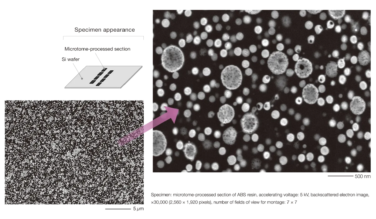
Low accelerating voltage, low vacuum and ultra-low magnification: stable, high-accuracy imaging of ABS resin at tens of thousands times magnification, high-brightness secondary electron images of gelatin, and slide-glass biological specimens such as artificial vessels observed from low to high magnification.
Specifications
| Specifications | JSM-IT710HR |
|---|---|
| Vacuum mode | Both high-vacuum (HV) and low-vacuum (LV) modes are included in the standard configuration |
| Resolution | For HV mode: 1.0 nm For LV mode: 1.8 nm For Analysis performance: 3.0 nm |
| Magnification | ×5 to ×600,000 |
| Electron gun | Schottky field emission gun |
| Accelerating voltage | 0.5 kV to 30 kV |
| Standard detectors | Secondary electron detector (SED) Backscattered electron detector (BED) |
| Energy dispersive X-ray spectrometer (EDS) (optional) | SD detector with detection surface area: 30/60/100 mm² can be installed |
| Automatic function | Beam alignment Focus / astigmatism / brightness / contrast correction |
| Major installable options | Low vacuum secondary electron detector (LVSED); Low vacuum hybrid secondary electron detector (LHSED); Energy dispersive X-ray spectrometer (EDS): SD detector with detection surface area: 30/60/100 mm²; Wavelength dispersive X-Ray spectrometer (WDS); Electron backscatter diffraction (EBSD); Load lock chamber (LLC); Stage navigation system (SNS); Chamber scope (CS); Operation panel; 3D analysis software |