
SEM — Model: JSM-IT210
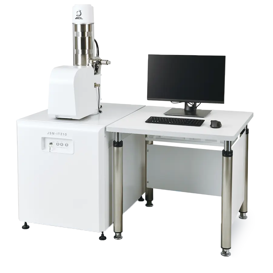
The JSM-IT210 is JEOL's most compact stationary scanning electron microscope, designed to make it easy to acquire data on all specimen types. Its newly developed stage is motor-driven on all five axes, making operation safer and faster.
Manufacturer: JEOL — Japan
Overview
The JSM-IT210 is JEOL's most compact stationary scanning electron microscope, designed to make it easy to acquire data on all specimen types. Its newly developed stage is motor-driven on all five axes, making operation safer and faster. The new "Simple SEM" function automatically acquires observation and analysis simply by selecting a field of view, making the JSM-IT210 a new-generation SEM that is compact and can be operated unattended.
Features
Specimen Exchange Navi
A guided workflow leads the operator from specimen exchange through to automatic observation.
- Set the specimen: Follow the on-screen Navi to set the specimen.
- Prepare during evacuation: Prepare for observation while the chamber is evacuating; a view inside the chamber makes searching for a field of view easy. (The chamber scope (CS) is optional.).
- Start observation automatically: Observation starts automatically. The stage navigation system (SNS) is optional; SNSLS is optional and can be used concurrently with SNS.
Zeromag: Magnify the Optical Image and Transition to the SEM Image
The Zeromag function simplifies navigation by providing a seamless transition from the optical image to the SEM image.
The SEM image, optical image and holder graphic are all linked for a global view of analysis locations. Optical image capture requires the stage navigation system (SNS, optional).
Live Analysis: Embedded EDS for Real-Time Elemental Composition
Live Analysis displays the EDS spectrum or element maps in real time during image observation, supporting searching and providing alerts for target elements.
The A (Analysis) or LA (Low Vacuum & Analysis) models are required.
Simple SEM: Automation for Enhanced Productivity
Simple SEM automates image collection at multiple locations, conditions and magnifications.
The workflow is: select observation conditions, set the target fields, then start automatic collection.
Tools for Speed
A stage with high positional accuracy lets you relocate analysis positions precisely.
Standard 60 mm² Large-Diameter EDS for Fast Analysis
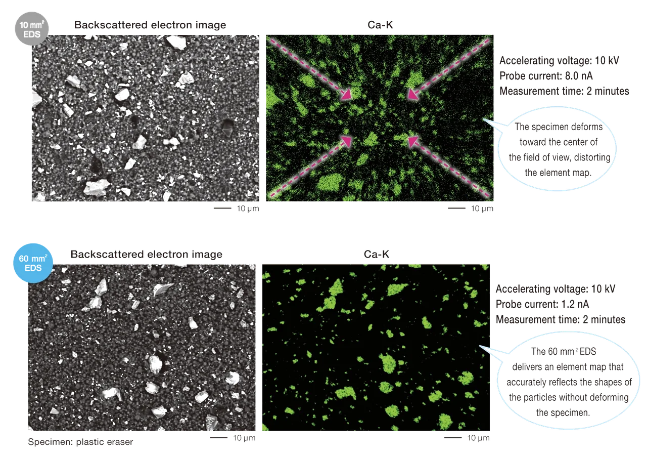
The 60 mm² sensor-size EDS fitted as standard on the JSM-IT210 obtains the same quality in far less time than smaller-area detectors, and performs multi-point analysis more efficiently. This EDS is compatible with the LV (Low Vacuum) and LA (Low Vacuum & Analysis) models.
- Fast Analysis: The 60 mm² EDS achieves the same result in about 10 seconds that a 10 mm² EDS needs 60 seconds to acquire.
- Application to Heat-Sensitive Specimens: A small-area EDS detector requires a large probe current for analysis, and heat-sensitive specimens can be damaged by beam irradiation, degrading the elemental map. The 60 mm² EDS collects an element map at lower probe current, enabling fast analysis while minimising heat damage.
- Fast, Clear Element Maps: The 60 mm² EDS produces a clear element map even with a one-minute measurement. Example: a pallasite meteorite mapped at 15 kV accelerating voltage in 1 minute, shown as a multi-colour overlay with individual Si-K, S-K, Fe-K and Ni-K maps alongside the backscattered electron image.
JSM-IT210 Series Configurations
The JSM-IT210 series can be equipped in the following four configurations:
- BU (Base Unit): Basic type, for observation under high vacuum.
- A (Analysis): Analysis type, with EDS included as standard.
- LV (Low Vacuum): Low vacuum type, for high vacuum and low vacuum observation, with BED included.
- LA (Low Vacuum & Analysis) Low vacuum and analysis type, with both BED and EDS included.
Specifications
| Specifications | JSM-IT210 |
|---|---|
| Resolution | High vacuum mode: 3.0 nm Low vacuum mode: 4.0 nm (BED) |
| Magnification | ×5 to ×300,000 |
| Electron gun | W filament, fully automatic gun alignment |
| Landing voltage | 0.3 to 30 kV |
| Probe current | 1 pA to 1 µA |
| Objective lens aperture | Four stages, with XY fine adjustment function |
| Energy dispersive X-ray spectrometer (EDS) (optional) | SD detector with detection surface area: 30/60/100 mm² can be installed |
| Automatic function | Filament adjustment, Gun alignment adjustment Beam alignment Focus / Astigmatism / Brightness / Contrast correction |
| Major installable options | Backscattered Electron Detector (BED); Low Vacuum Secondary Electron Detector (LVSED); Low Vacuum Hybrid Secondary Electron Detector (LHSED); Energy dispersive X-ray spectrometer (EDS): SD detector with detection surface area: 30/60/100 mm²; Stage Navigation System (SNS); Chamber Scope (CS); Operation Panel (OP2); 3D Analysis Software (SVM) |