
MultiBeam FIB-SEM — Model: JIB-PS500i
The JIB-PS500i provides three solutions to assist TEM specimen preparation. High throughput workflow is assured from specimen prepartion to TEM observation.
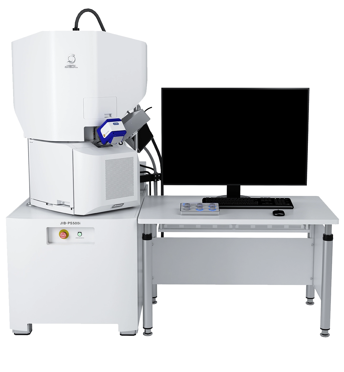
Manufacturer: JEOL — Japan
Overview
New Solutions for Specimen Preparation.
The JIB-PS500i is a FIB-SEM system that provides three solutions to assist TEM specimen preparation, assuring a high-throughput workflow from specimen preparation through to TEM observation. Its strengths span cutting-edge preparation, imaging, and analysis.
TEM - Linkage
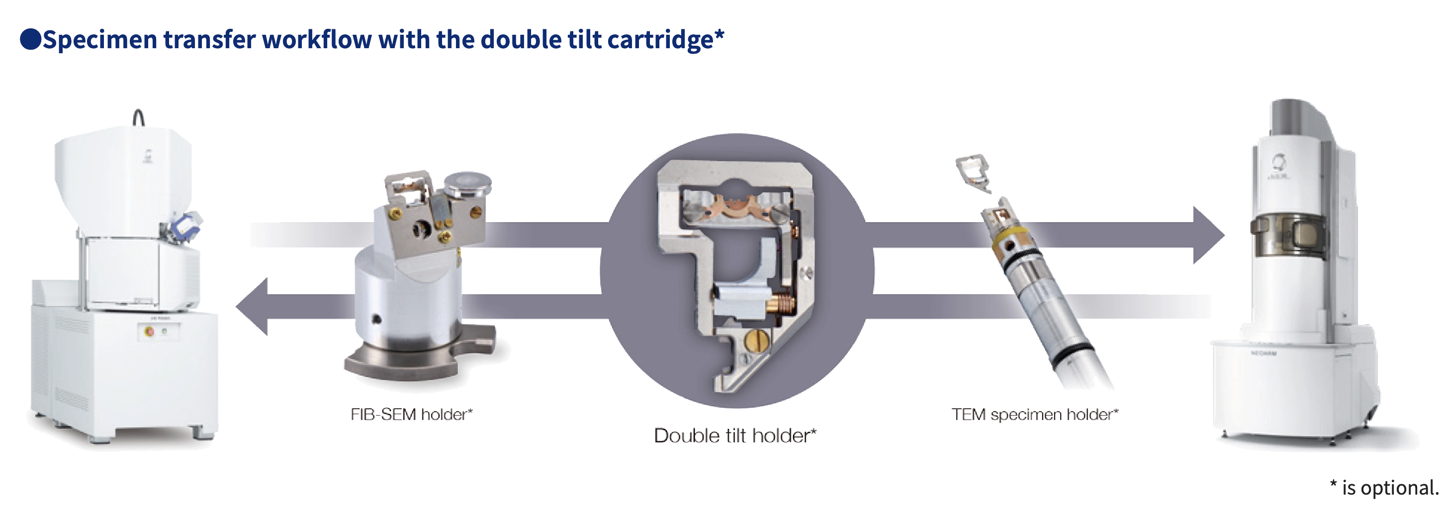
JEOL's double-tilt cartridge and TEM holder (optional) facilitate linkage between the TEM and the FIB. The cartridge can be attached to the dedicated TEM specimen holder with a single touch.
Specimen transfer workflow with the double-tilt cartridge (optional)
The optional double-tilt cartridge streamlines the specimen transfer workflow from the FIB to the TEM.
OmniProbe 400 (optional)
The adopted OmniProbe 400 (Oxford Instruments) enables precise, smooth pick-up operations and manipulations. Its operations are integrated into the JIB-PS500i software.
Check - and - Go
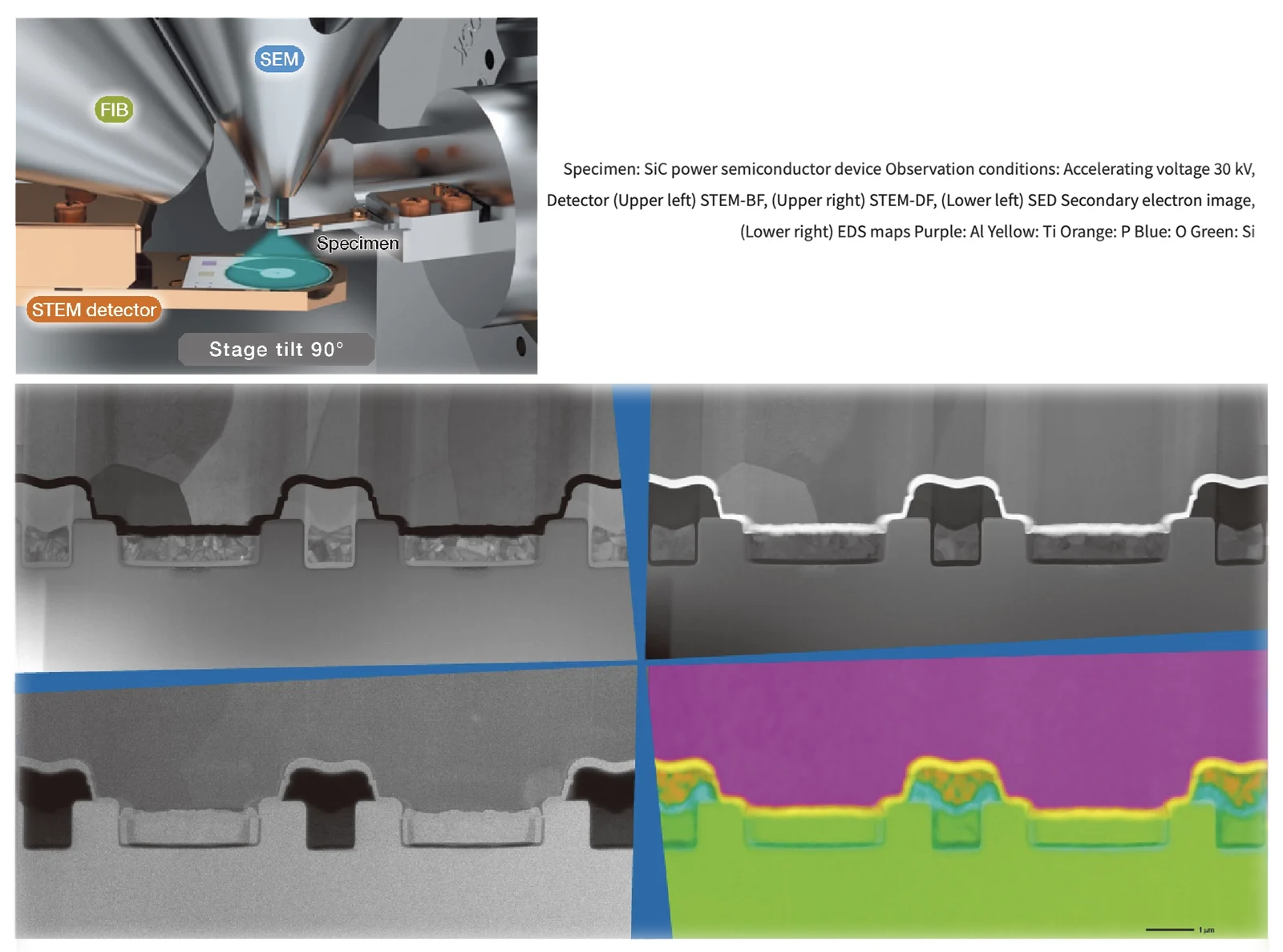
To precisely and efficiently prepare a TEM specimen, it is essential to quickly check the preparation progress. With its high-tilt stage and detector scheme, the JIB-PS500i allows seamless transition from FIB milling to scanning transmission electron microscope (STEM) imaging. Fast transitions between lamella processing and STEM imaging lead to efficient specimen preparation.
Automatic Preparation
The JIB-PS500i automates specimen preparation using the STEMPLING2 automatic TEM specimen preparation system (optional). This automatic system enables any operator to smoothly prepare specimens for TEM.
High-Resolution & High-Contrast SEM Imaging
Stop hesitating and stop missing the end-point in milling - high-quality SEM images assist you.
Signal detection system
Multiple detectors are available, including the standard SED, UED, and iBED. Selecting the optimum detector makes it possible to observe sharp images of various specimens under various experimental conditions.
High-resolution SEM imaging
A newly developed super conical lens system is built into the SEM column, greatly improving imaging performance at low accelerating voltage. This superb imaging is very useful for checking the end-point milling status of a lamella specimen using the SEM.
SEM imaging of FIB-prepared cross section
A very small, retractable backscattered electron detector (RBED, optional) can be used even at high stage tilt. For imaging of a FIB-prepared cross section - which requires both specimen-surface and tilted imaging - a combination of various detectors including the SED and UED makes the system suitable for cross-sectional SEM imaging.
EDS integration software (optional)
EDS analysis functions are built into the main instrument control software, enabling elemental analysis of the specimen without switching software. This is available only when the instrument is equipped with a JEOL EDS (optional).
High-Power & High-Quality FIB Processing
For the best specimen preparation, more powerful FIB processing.
Large-area, fast FIB processing
The FIB column enables processing with a large-current Ga ion beam (up to 100 nA). This high-current processing is particularly effective for large-area imaging and analysis.
Damage-layer removal by low-kV processing
The FIB column is set to a shorter working distance than JEOL's previous models; combined with a new power supply, this greatly improves processing performance at low accelerating voltages. The addition of a new control system yields the high-performance fine-milling capabilities essential for quality lamella preparation.
New Chamber & Stage Design
A highly flexible, high-tilt, large stage to meet any requirement.
Loading a large specimen
The JIB-PS500i adopts a large specimen chamber and a newly developed 5-axis full-eucentric large-motor stage, increasing the stage movement range while accommodating a large specimen. This large stage allows processing and imaging of the entire surface of a specimen 130 mm in diameter, and a sample up to 80 mm in height can be loaded into the specimen chamber. A silicon wafer 150 mm in diameter can be loaded into the specimen chamber.
AVERT Engine to determine movement limit using 3D models
The AVERT Engine determines the specimen movement limit using 3D models of the specimen holder, stage, and objects inside the chamber. Under any condition, the specimen cannot interfere with the detector or the objective lens.
Specifications
| Specifications | JIB-PS500i |
|---|---|
| SEM Specifications | |
| Image resolution | 0.7 nm (15 kV) 1.4 nm (1 kV) 1.0 nm (1 kV, BD mode) |
| Magnification | ×50 to ×1,000,000 (STD mode) ×1,000 to ×1,000,000 (UHR mode) ×10 to ×19,000 (LDF mode) (128 mm × 96 mm print size) |
| Landing voltage | 0.01 to 30 kV |
| Beam current | ~1 pA to 500 nA or more |
| Specimen bias voltage | 0.0 to -5.0 kV |
| Electron gun | In-lens Schottky Plus field emission electron gun |
| Aperture angle control lens (ACL) | Built-in |
| Objective lens | Power stabilization lens |
| Long depth of focus (LDF) mode | Built-in |
| Detector (standard) | Secondary electron detector (SED), Upper electron detector (UED), In-lens backscattered electron detector (iBED) |
| FIB Specifications | |
| Image resolution | 3 nm (at 30 kV) |
| Magnification | ×50 to ×300,000 (limited depending on accelerating voltage) |
| Accelerating voltage | 0.5 to 30 kV |
| Beam current | 1.0 pA to 100 nA, 13 stages switchable (30 kV) |
| Movable aperture | Motor drive, 16 stages switchable (3 stages are auxiliary) |
| Ion source | Ga liquid metal ion source |
| Processing shapes by milling | Rectangle, Circle, Polygon, Spot, Line, BMP |
| Specimen Stage Specifications | |
| Type | Full eucentric goniometer stage |
| Control | Computer control, 5-axis motor control, 3D interference measurement AVERT Engine |
| Specimen movements | X: 130 mm Y: 130 mm Z: 1.0 mm to 40 mm Tilt: -40.0 to 93.0° Rotation: 360.0° endless" |