
EPMA — Model: JXA-iSP100
JXA-iSP100 integrated with enhanced features, satisfies the needs of research development & quality assurance in a variety of fields and achieves efficient operations from observation to analysis.
Enables observation of surface tissues and morphology and local trace element analysis.
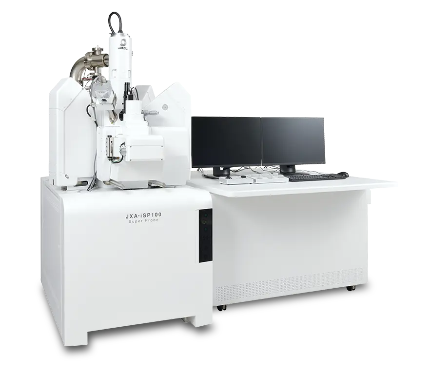
Manufacturer: JEOL — Japan
Overview
The Electron Probe Microanalyzer (EPMA) is an established tool for research, development and quality assurance across industries such as steel, automotive, electronic components and battery materials, and its applications continue to expand. In academia, EPMA is widely used in earth and planetary science and materials science, with growing contributions expected in advanced research on minerals, energy materials and new materials. What these users increasingly demand is an instrument that is simpler and faster to use - accessible to anyone - without compromising the high performance of microanalysis.
JXA-iSP100 integrated with enhanced features, satisfies these needs of research development & quality assurance and achieves efficient operations from observation to analysis.
Effortless Setup
Holder Insertion with Auto Loading
Specimen insertion and acquisition of an optical image of the specimen holder (Stage Navigation image) are executed with a single click. The field for analysis can then be selected directly from the Stage Navigation image, so you can quickly find the target observation point.
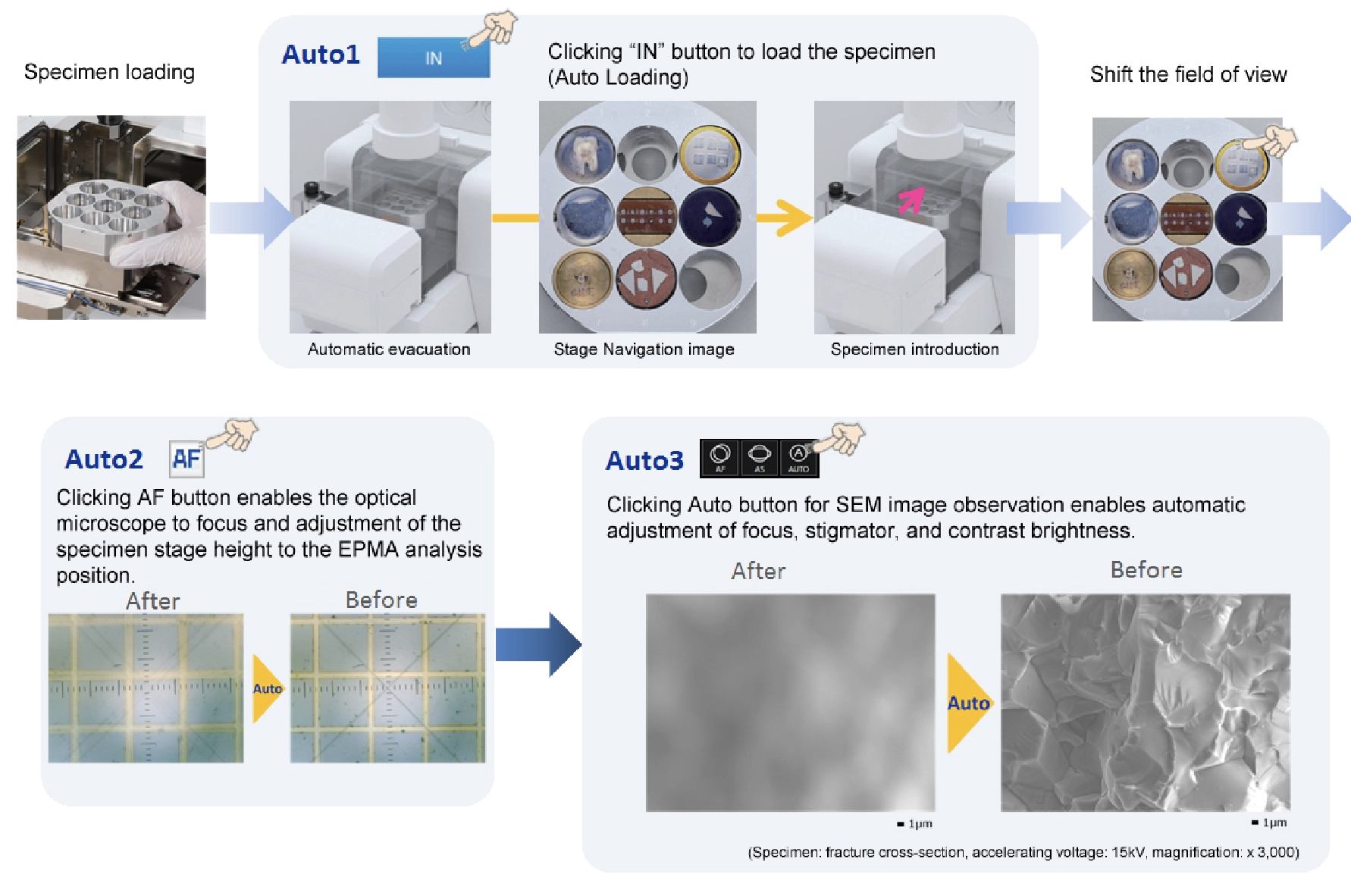
Simplified Analysis
By combining the Auto Focus function of the optical microscope with a new, more accurate and faster generation of SEM Auto functions, any user can acquire high quality SEM images. Operability is further enhanced through the integration of SEM, EDS, WDS and optical images.
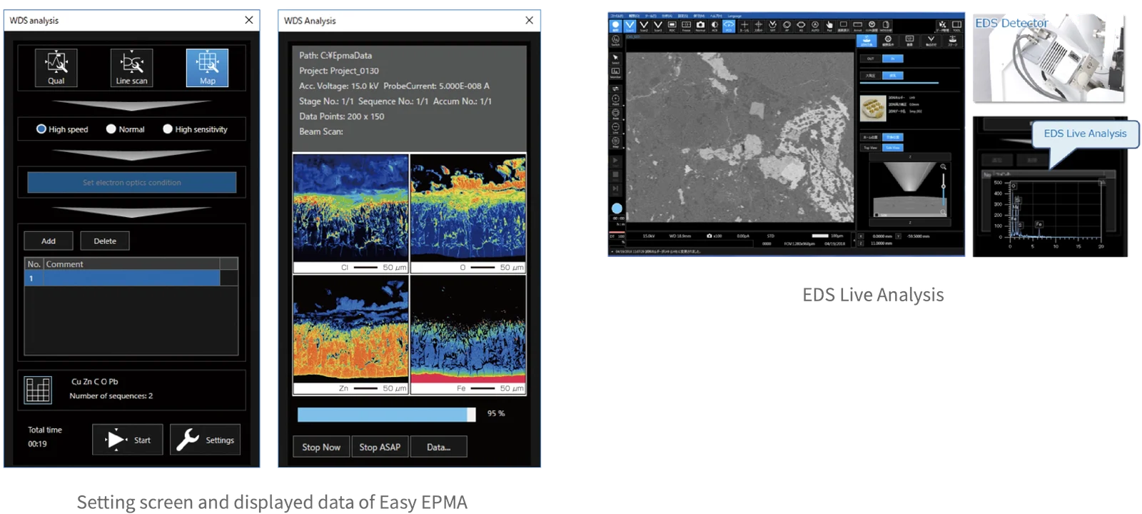
Live Analysis
Live Analysis enables elemental screening while you are still observing the specimen, so preliminary composition information is available during imaging.
Easy EPMA
With Easy EPMA, instrument settings are simplified for fast elemental analysis, allowing even novice users to operate the EPMA smoothly.
EPMA-XRF Integration and WD/ED Integration
EPMA-XRF integration allows analysis conditions of the EPMA to be set based on XRF data, while integration of WD and ED spectrometry shortens overall analysis time. A single click sets the analyzing-crystal combination based on the elements recommended from these techniques.
Self Maintenance
Efficient Calibration with 18 Built-in Standard Specimens
A new spectrometer calibration function reduces the steps involved in periodic calibration and eliminates mis-operation by using 18 built-in standard specimens. Automated instrument calibration can be run overnight for greater efficiency.
Maintenance Notification
The maintenance notification function, provided through the Customer Support Tool, ensures that proper maintenance is carried out at the required timing.
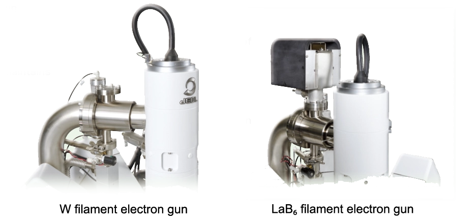
Electron Gun
W-Filament Electron Gun
Detection of trace elements in a short time with high current analysis.
Easy maintenance, for simple replacement of a gun filament.
The beam stabilizer provided in the standard configuration maintains current stability over long periods.
Max. probe current: 10 μA.
Probe current stability: ±0.05% / h; ±0.3% / 12 h.
LaB₆ Electron Gun (Option)
Unavoidable filament replacement during long acquisition of elemental maps is reduced.
Single crystal, long-life LaB₆ tip.
Easy maintenance, for simple replacement of a gun filament.
No baking required after filament replacement.
Unlike the W-gun, large probe currents and high spatial resolution are achieved at low accelerating voltages.
The LaB₆ filament can easily be interchanged with a W filament.
Related Option: Soft X-ray Emission Spectrometer (SXES)
The Soft X-ray Emission Spectrometer (SXES) is an ultra-high resolution spectrometer built around a newly developed diffraction grating and a high-sensitivity X-ray CCD camera. Like EDS it offers parallel detection, and it performs ultra-high energy resolution analysis of 0.3 eV (Fermi-edge, Al-L standard), surpassing the energy resolution of WDS.
Specifications
| Specifications | JXA-iSP100 |
|---|---|
| Detectable element range | WDS: Be*¹ / B to U, EDS: Be to U |
| Detectable X-ray range | Detectable wavelength range with WDS: 0.087 to 9.3 nm Detectable energy range with EDS: 20 keV |
| Number of spectrometers | WDS: Up to 5 selectable, EDS: 1 |
| Maximum specimen size | 100 mm × 100 mm × 50 mm (H) |
| Electron gun | W- filament /LaB₆*² |
| Accelerating voltage | 0.2 to 30 kV (0.1 kV steps) |
| Probe current range | 1 pA to 10 µA |
| Probe current stability | ± 0.05% / h (W), ± 0.3% / 12 h (W) *³ |
| Resolution (secondary electron image) | 6 nm (W) 5 nm (LaB₆)³ |
| Scanning magnification | ×40 to 300,000 (W.D. 11 mm) |
| Notes | *¹ With analyzing crystal for Be analysis. *² LaB₆ is an option. *³ Room temperature variation: less than ± 0.5 ℃ |