
200 kV TEM — Model: JEM-F200
The JEM-F200 is a field emission transmission electron microscope, which features higher spatial resolution and analytical performance coupled with intuitive user interface for multi-purpose operation.
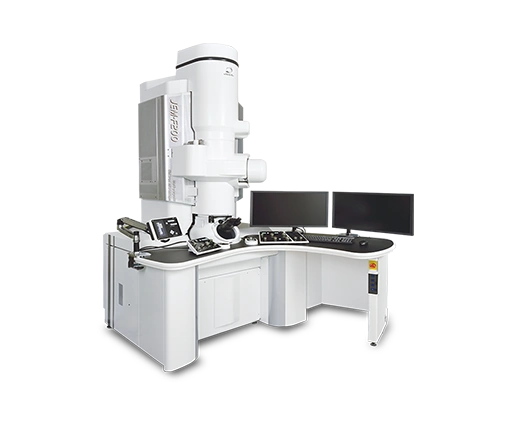
Manufacturer: JEOL — Japan
Overview
The JEM-F200 is a field emission transmission electron microscope, which features higher spatial resolution and analytical performance coupled with intuitive user interface for multi-purpose operation.
JEM-F200 is the only multipurpose, high-throughput, 200 kV TEM in its class to offer a Cold Field Emission Gun and dual Silicon Drift Detectors.
The boost in probe current from the Cold FEG combined with dual EDS detectors makes the JEM-F200 a top performance analytical TEM.
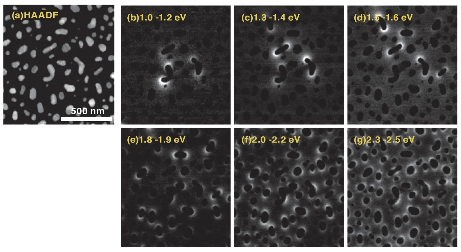
The high brightness/narrow energy spread of the next-generation JEOL Cold-FEG achieves high energy resolution Electron Energy Loss Spectroscopy (EELS) for rapid identification of chemical bonding states.
Dual Silicon Drift Detectors (SDD) offer the ultimate high sensitivity and throughput for X-ray analysis.
Additionally, the new Advanced Scan System employs De-Scan to achieve wide-field STEM-EELs spectrum imaging.
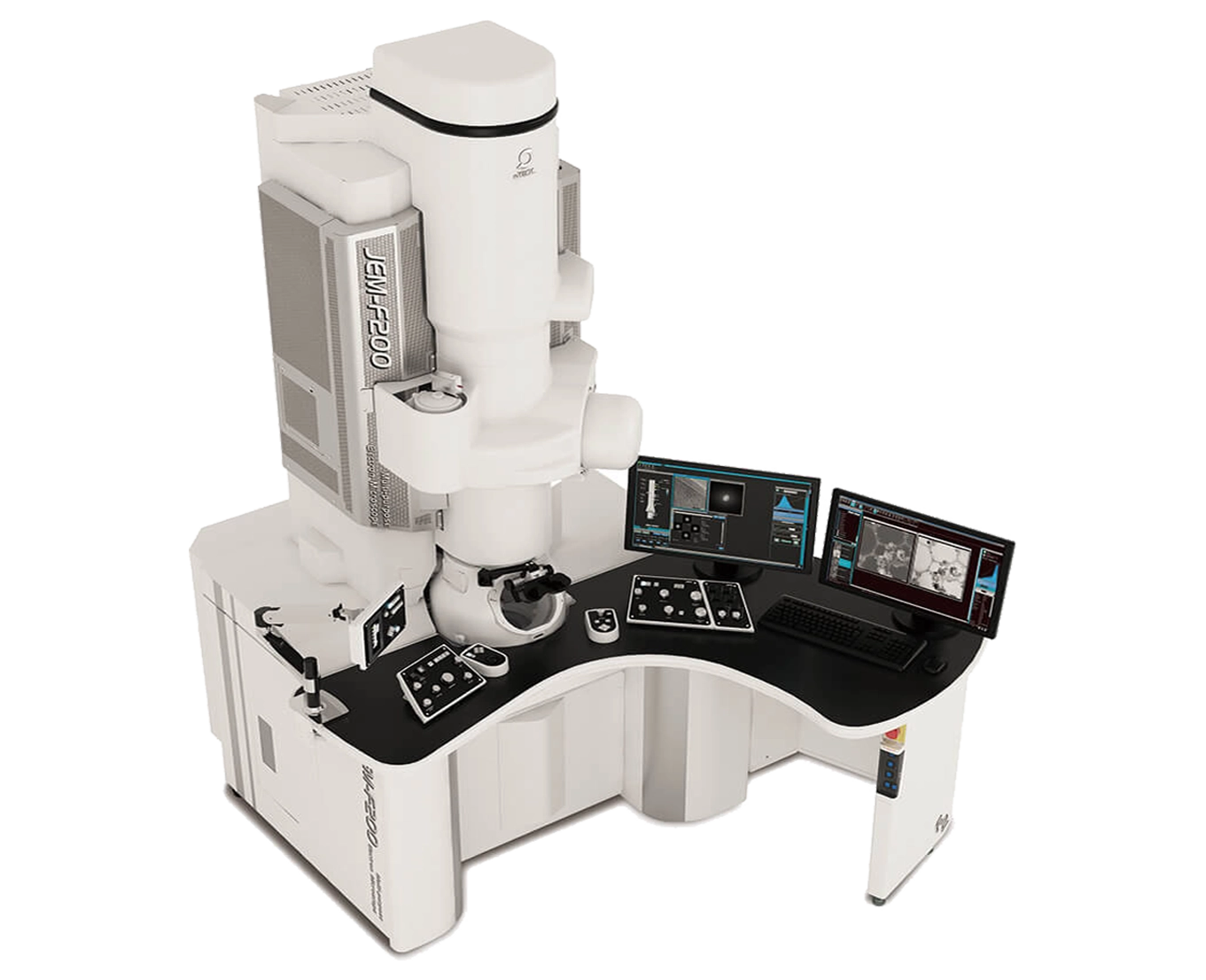
Features
High-resolution TEM/STEM observations from high to low acceleration voltages
The JEM-F200 offers a cold field-emission electron gun, which guarantees high stability, high brightness, and high energy resolution (<0.33 eV).
This electron gun effectively achieves higher-resolution imaging by minimizing chromatic aberrations originating from the energy spread of the electron source.
Furthermore, by incorporating JEOL's 10+ years of expertise into the design, we have significantly improved both mechanical and electrical stability.
High-throughput and high-accuracy EDS analysis
The JEM-F200 can be equipped with two large-area Silicon Drift Detectors (SDD) simultaneously, providing high-sensitivity analysis.
The large area and high sensitivity enables efficient EDS analysis at a fraction of the time with reduced damage.
Additionally, utilizing high-speed, lossless drift correction via live STEM images during EDS mapping enables efficient measurements while reducing sample damage from the electron beam.
EELS analysis with high energy resolution
The CFEG of the JEM-F200 can obtain analysis of chemical bonding states and electronic structure at high energy resolution, surpassing the capabilities of a Schottky field emission electron gun.
This is made possible by incorporating a cold field-emission electron gun that guarantees high energy resolution (<0.33 eV) with EELS (option).
Easy operation with minimal stress even for beginners
The JEM-F200 is equipped with an intuitive user interface that emphasizes user-friendliness.
It offers comprehensive auto functions for both TEM and STEM, making it easy for beginners to operate.
Additionally, to facilitate easy insertion and removal of sample holders, SPECPORTER™ is incorporated, which enables safe and automated sample holder insertion.
Moreover, the sample stage is equipped with a Pico stage, drive, enabling precise picometer-level movement without requiring a piezo drive mechanism.
This allows for a wide range of field-of-view adjustments, from the entire sample mesh to atomic-level imaging.
Seamless workflow from FIB sample preparation to TEM/STEM imaging
A double tilt cartridge and dedicated TEM holder facilitates linkage between TEM and FIB operations.
The cartridge easily transfers between the FIB holder and TEM sample holder with a single touch, eliminating the need to handle a TEM lamella after processing.
FEMTUS™ Integrated Analysis Platform
The newly developed FEMTUS™ Integrated Analysis Platform enables the centralized management and processing of a wide range of data obtained from the various detectors embedded in the transmission electron microscope. The GUI has a simple layout that is easy to use for both beginners and advanced users.
Transmission Electron Microscope for a Sustainable Society
The JEM-F200 is the first transmission electron microscope to standardly incorporate an ECO mode. This mode efficiently maintains the instrument with minimal energy consumption during periods of non-use, saving energy.
Activating the ECO mode reduces energy consumption to approximately one-fifth of that during normal operation, contributing to a more sustainable society.
Additionally, it features a scheduling function, allowing the instrument to return to a usable state from ECO mode at specified dates and times.
Two Configurations
The JEM-F200 offers two (02) configurations:
- JEM-F200(UHR) - is the ultra high resolution configuration.
- JEM-F200(HR)- is the high resolution configuration.
Typical Applications
Semiconductor Device Analysis
An HAADF-STEM image of a FinFET sample thinned with JEOL's focused ion beam (JIB-PS500i) shows a clear lattice image over a region of 200 nm or more on the silicon substrate (accelerating voltage 200 kV, STEM mode, 1.0 M magnification). The JEM-F200 demonstrates excellent performance in microstructural analysis of semiconductors due to its high resolution and contrast, and EDS/EELS mapping resolves O, N, Si, Ti, W, Al, Ge and Hf distributions in MOS transistor structures.
Materials Science
Examples include TEM dark-field imaging of Al alloys, STEM-OBF imaging of zeolites, STEM-EDS, BF and ADF imaging of garnet at atomic resolution, HAADF/OBF imaging of amphibole, and atomic resolution electric field observation of Si₃N₄ using a segmented semiconductor STEM detector.
Biological Samples
TEM imaging of biological samples such as spleen tissue, with automated functions and SPECPORTER™ holder transfer supporting cryoholder workflows.
Specifications
| Specifications | JEM-F200(UHR) | JEM-F200(HR) |
|---|---|---|
| Electron gun | Cold field emission electron gun (CFEG) Schottky field emission electron gun (TFEG) | |
| Accelerating voltage | 20 to 200 kV (200 kV and 80 kV are supported as standard, other values are optional) | |
| TEM resolution (at 200 kV) | Lattice image: 0.19 nm Particle image: 0.1 nm Information limit: ≦0.11 nm (with CFEG) ≦0.12 nm (with TFEG) | Lattice image: 0.23 nm Particle image: 0.1 nm Information limit: ≦0.11 nm (with CFEG) ≦0.12 nm (with TFEG) |
| STEM resolution (at 200 kV) | Dark-field STEM image: 0.14 nm (CFEG) 0.16 nm (TFEG) | |
| Sample movement ¹ | X, Y: ±1.0 mm, Z: ±0.1 mm | X, Y: ±1.0 mm, Z: ±0.2 mm |
| Sample tilt angle ¹ | Double-tilt holder TX / TY: ±25°/±25° High-tilt holder TX: ±60° | Double-tilt holder TX / TY: ±35°/±30° High-tilt holder TX: ±80° |
| EDS (optional) | 2 units of SDDs of detection surface area 100 mm² can be installed. Resolution ≦ 129 eV for Mn Kα. Output count rate: 10 kcps. | |
| EDS solid angle | SDD1: 0.6 sr / SDD2: 0.6 sr | SDD1: 1.0 sr / SDD2: 0.7 sr |
| Vacuum evacuation system | Sputter ion pump, oil diffusion pump, oil rotary pump | |
| Major installable Options | Scanning bright-field electron detector; Scanning bright-field aperture; Backscattered electron detector; FEMTUS™ Integrated Analysis Platform; Energy-dispersive X-ray spectroscopy (EDS); Electron energy-loss spectroscopy (EELS); Digital Camera (JEOL CMOS camera); TEM/STEM/EDS Tomography System; Dry pump unit (SIP, TMP, RBP) | |
| Notes | ¹ The movable range is subject to change depending on the sample holder type and the presence/absence of the objective aperture. |