
200 kV TEM — Model: JEM-ARM200F NEOARM
The JEM-ARM200F NEOARM is an atomic resolution analytical electron microscope, powered by the "Neo Engine". It combines JEOL's unique cold field emission gun (Cold FEG) with a new Cs corrector (ASCOR) that compensates for higher-order aberrations.
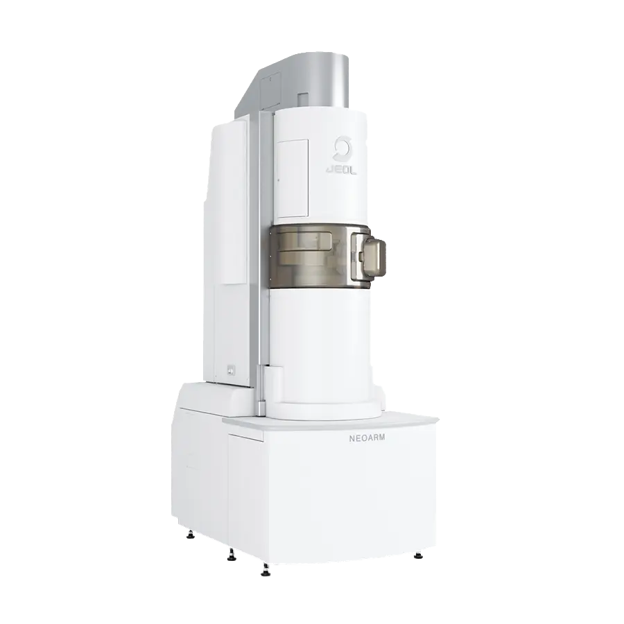
Manufacturer: JEOL — Japan
Overview
The JEM-ARM200F NEOARM is an atomic resolution analytical electron microscope, powered by the "Neo Engine". It combines JEOL's unique cold field emission gun (Cold FEG) with a new Cs corrector (ASCOR) that compensates for higher-order aberrations. The combination of Cold FEG and ASCOR enables atomic-resolution imaging not only at 200 kV accelerating voltage but also at a low voltage of 30 kV.
NEOARM is also equipped with an automated aberration correction software JEOL COSMO™ incorporating JEOL's new aberration correction algorithm for fast, precise and automatic correction, enabling higher-throughput atomic-resolution imaging.
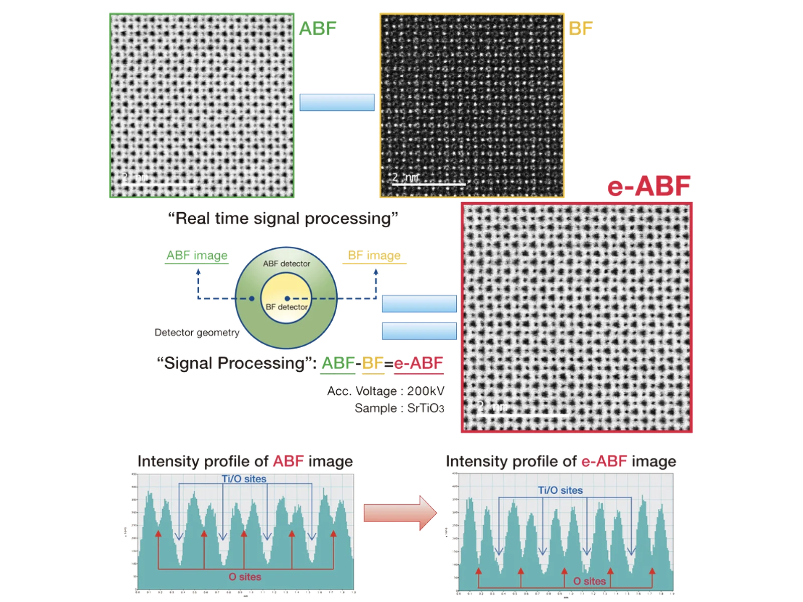
A new STEM detector providing enhanced contrast of light elements is incorporated as standard. Light-element contrast enhancement is achieved by a new STEM imaging technique e-ABF, facilitating observation of light-element materials even at low accelerating voltages.
The microscope room is separated from the operation room to respond to a remote operation.
Features
Spherical Aberration (Cs) Corrector ASCOR
ASCOR (Advanced STEM Corrector) incorporated in "NEOARM" can suppress the six-fold astigmatism which limits resolution after Cs correction.
The combination of ASCOR and Cold FEG gives low chromatic aberration and expands the diffraction limit, achieving higher resolution than ever.
Automatic Aberration Correction Software JEOL COSMO™
JEOL COSMO™ (Corrector System Module) adopts a new aberration correction algorithm (SRAM: Segmented Ronchigram Auto-correlation function Matrix). Thus, no special sample is required for aberration correction, leading to high-precision and quick correction of higher order aberrations. This system enables fast processing compared to the conventional correction algorithm and also automates the operations, thus eliminating a complicated correction workflow in the customer microscope. These features enable higher-throughput atomic-resolution imaging.
New ABF Detector System
The ABF (Annular Bright Field) detector is widely used as a technique suitable for high-resolution imaging of light elements. "NEOARM" supports enhanced contrast of light elements by a newly-designed ABF imaging technique e-ABF (enhanced ABF).
This capability facilitates atomic-level structure observation of materials containing light elements.
Perfect Sight Detector
The perfect sight detector integrated into NEOARM uses hybrid scintillators, always enabling the acquisition of high-contrast, quantitative STEM images irrespective of the accelerating voltage setting.
OBF STEM System (Option)
In the OBF (Optimum Bright Field) STEM imaging method, raw images acquired by a segmented STEM detector are used as the source for a phase image reconstruction, with dedicated Fourier filters to maximize the signal to noise ratio of retrieved image.
This promising method realizes higher contrast for both heavy and light elements even while operating under extremely low electron dose conditions. Beam sensitive materials difficult to observe with standard ADF and ABF STEM methods can be easily analyzed with higher contrast at a wide range of magnifications.
STEM Low-Dose Imaging
The beam sensitive materials including Metal Organic Frameworks (MOFs) and Zeolites require a reduced electron dose (typically, probe current < 1.0 pA) while maintaining clear atomic contrasts for the framework of light elements.
The OBF STEM has an advantage for such low dose experiments, realizing ultra high dose-efficient STEM imaging in an atomic resolution.
Both of OBF STEM Image MOF MIL-101(left) and MFI Zeolite (right) are acquired in a single shot and the high spatial resolution of 1 Å can also be observed on the FFT pattern in right inset. Moreover, stack image averaging (left inset) confirms that resolution and contrast are very well balanced.
High-Contrast Imaging of Light Elements
In addition to being highly dose efficient, OBF STEM is also advantageous for light element imaging.
Even in a lower acceleration voltage, both higher contrast and spatial resolution can be achieved for light elements.
The resolution for light elements becomes much better with a higher acceleration voltage.
Each atomic column is now clearly separated with a deep sub-angstrom resolution inside complex structures or along higher-index crystallographic axes.
The quality of OBF STEM is excellent in low dose conditions, and further enhanced under the standard probe conditions of a Cs-corrected electron microscope.
Live OBF Imaging
In an actual experiment, live OBF imaging is fundamental for beam sensitive materials as all operations should be performed in a dose limited condition. The live function is included in the OBF system, implemented within the TEM control software, with simple GUI control and real time display updates alongside conventional STEM images.
Specifications
| Specifications | JEM-ARM200F NEOARM |
|---|---|
| Resolution (with STEM/TEM Cs corrector configured) | STEM HAADF image: 70 pm (200 kV), 100 pm (80 kV), 160 pm (30 kV) TEM information limit: 100 pm (200 kV), 110 pm (80 kV), 250 pm (30 kV) |
| Electron gun | Cold field emission gun (Cold FEG) [standard configuration] |
| Aberration corrector | STEM: NEO ASCOR HOAC (Higher order aberration corrector) TEM: CETCOR with DSS (DeScan system) |
| Corrector auto tuning system | NEO JEOL COSMO™ Auto tuning system Ad-hock tune (SIAM) built-in |
| Accelerating voltage | 30 to 200 kV (80, 200 kV: standard, 30, 60, 120 kV: optional) |
| Magnetic field free mode | Lorentz lens settings (×50 to 80 k on screen) [standard configuration] |
| Specimen movement system | X, Y and Z super-fine mechanical drive, ultra-fine piezo device drives: standard |
| Operation type | RDS (Room divided style) operation |