
200 kV TEM — Model: JEM-2100Plus
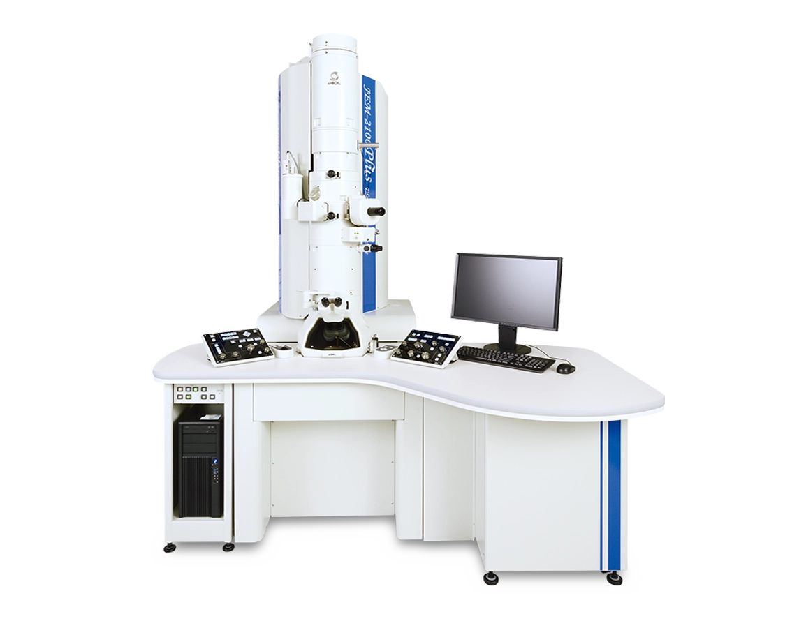
The JEM-2100Plus is a multi-purpose transmission electron microscope developed as a successor of the JEM-2100 general-purpose electron microscope. It combines the proven JEM-2100 optical system with an advanced control system and versatile functions for further improved ease of use.
Manufacturer: JEOL — Japan
Overview
The JEM-2100Plus is a multi-purpose transmission electron microscope developed as a successor of the JEM-2100 general-purpose electron microscope.
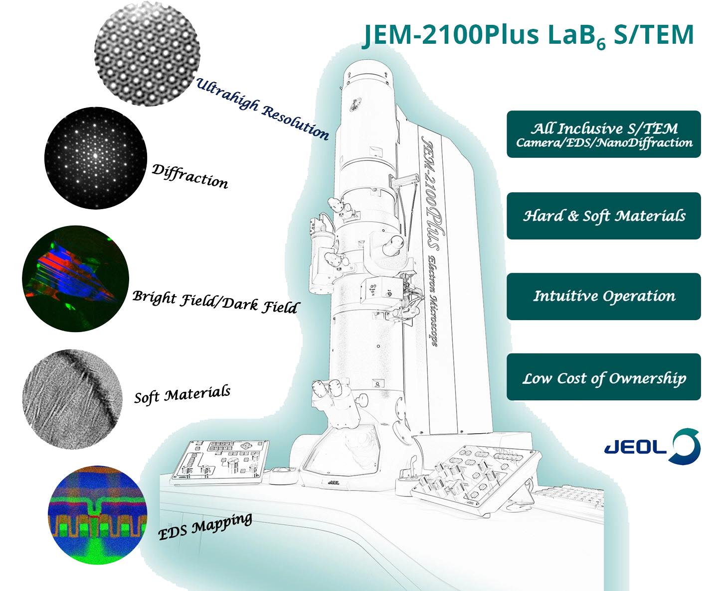
It combines the proven JEM-2100 optical system with an advanced control system and versatile functions for further improved ease of use. Key features include a new design and user interface, the advanced operation software "TEM Center", integration with a high pixel-resolution camera and STEM, a complete range of User Assist functions, and offline image viewing/editing software.
New Design and User Interface
The JEM-2100Plus reduces the width of the main instrument by approximately 22 cm compared to the JEM-2100, making the layout space wider in the installation room.
The column cover has been redesigned with a streamline shape and the work table is made left-right asymmetric, broadening the workspace around the microscope. A 24-inch wide monitor completes the operator station, and the control panels feature improved knob material and button colors for better operability and visibility, with a new STEM-image adjustment knob positioned on the right panel so the specimen can be tilted using a dedicated panel.
Advanced Operation Software "TEM Center"
The advanced operation software "TEM Center" compactly positions the buttons that operate the TEM column in a task bar to the left, so the operator is not asked to open extra windows. When detailed operations are needed, clicking the links for each item displays the corresponding windows, enabling intuitive and simple operation compared to conventional microscopes.
Integration with High Pixel-Resolution Camera
Installation of a JEOL-made bottom-mount camera enables camera operation and image acquisition through the TEM Center. Two types are available: the high pixel-resolution CCD camera "Ruby" with 8 M pixels, and the "Matataki Flash" camera with a cutting-edge sCMOS sensor. Both cameras meet a variety of needs such as acquisition of TEM images and diffraction patterns, and bright-field and dark-field images whose brightness and contrast are greatly different are also acquired with high pixel-resolution.
Integration with STEM
The STEM operation screen is also integrated into the TEM Center: a single click of the button switches TEM mode to STEM mode. A wealth of automatic functions — auto save, auto focus, auto contrast & brightness — allows novice users to easily operate the microscope, and the new Ronchigram mode enables smooth alignment of the STEM image. Scan rotation and adjustment of STEM-image intensity and contrast can be made using the control panel as well as from the GUI.
A Complete Range of User Assist Functions
Stage Navigation
Clicking on a saved image automatically moves the stage to the indicated location, allowing the operator to navigate to the area of interest without changing the magnification, even at high magnification.
Digital Montage
A single button controls fully automated operation from image acquisition to stitching. Brightness and contrast are automatically adjusted, resulting in a single image with no visible stitching. Acquisition of high pixel-resolution, wide-area images lets you confirm fine structures even at high magnification.
Drift Correction by Image Integration
The JEM-2100Plus comes with a function to perform image integration while correcting image drift, so a sharp image with no image blur is acquired.
"SightX Viewer" Offline Image Viewing/Editing Software
SightX Viewer enables offline examination and editing of TEM or STEM images acquired with the microscope. Installed on an arbitrary PC, it provides image viewing and editing in the same manner as the TEM Center, with an image-display window (montage images can also be examined), histogram window, thumbnail window, and measurement tools.
STEM Imaging
Scanning transmission electron microscopy (STEM) scans a finely-focused electron beam over a specimen and forms an image by detecting the intensities of electrons passing through the specimen. A bright-field image (STEM-BF) formed by transmitted electrons and a dark-field image (STEM-DF) formed by scattered electrons are observed.
TEM/STEM Tomograph
The JEM-2100Plus can accommodate the TEM/STEM Tomograph System that automates electron tomography. This unique Tomograph System consists of three components that enable you to acquire three-dimensional (3D) images with simple operation:
Recorder — acquires the series of tilt images required for 3D reconstruction of TEM or STEM images.
Composer — performs 3D reconstruction based on the series of tilt images acquired with the TEM.
Visualizer-kai — displays the reconstructed 3D data in various ways.
EDS Analysis
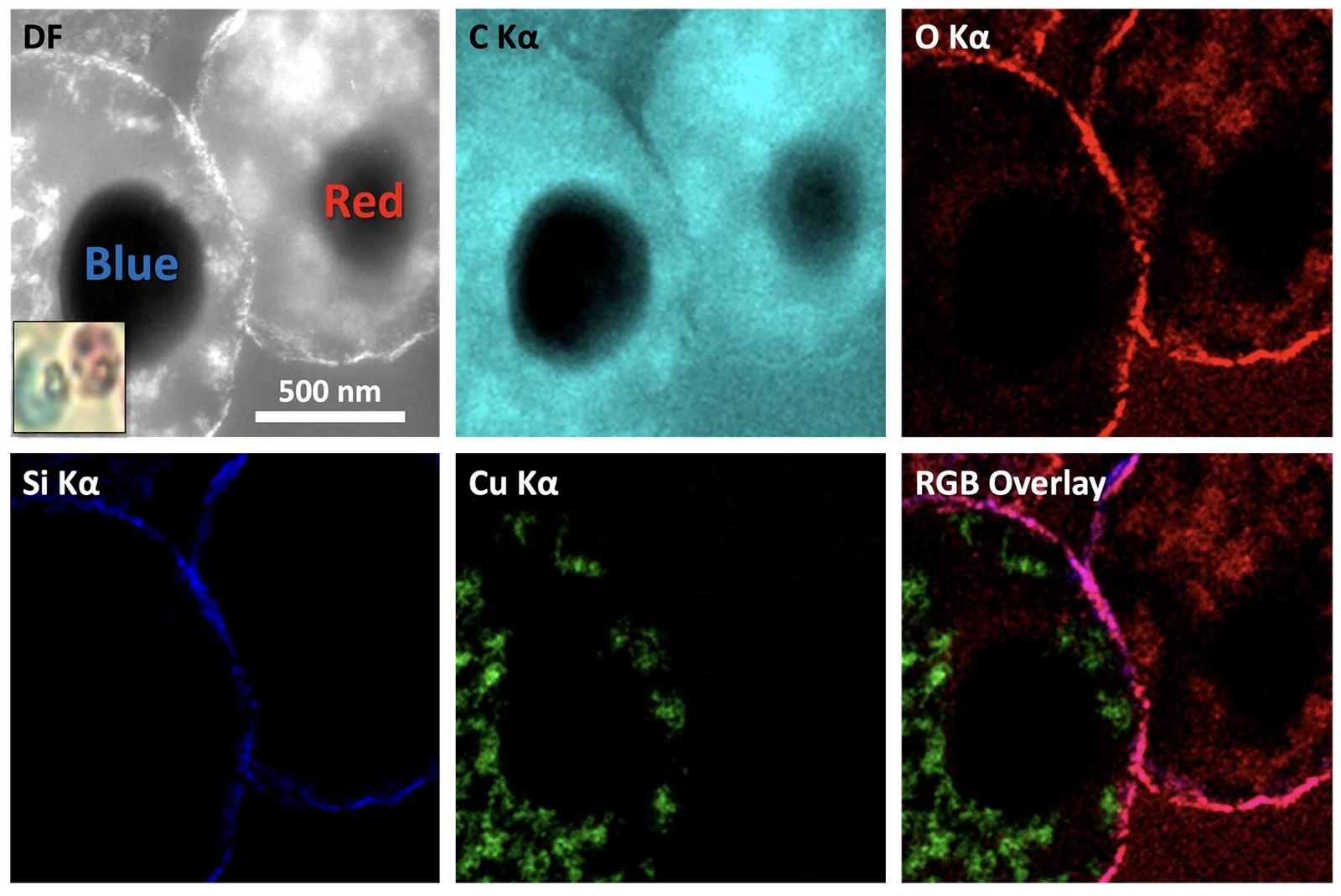
Energy Dispersive X-ray Spectroscopy (EDS) enables simultaneous analysis of a wide range of elements from Be to U. Combination with STEM extends its application fields, ranging from point analysis to element mapping.
Five Configurations
The JEM-2100Plus offers five (05) configurations:
- JEM-2100Plus(UHR) - is the ultra high resolution configuration.
- JEM-2100Plus(HR)- is the high resolution configuration.
- JEM-2100Plus(HT)- is the high specimen tilt configuration.
- JEM-2100Plus(CR) - is the crto polepiece configuration.
- JEM-2100Plus(HC) - is the high contrast configuration.
Typical Applications
Life Science
High pixel-resolution imaging of biological specimens such as rat hippocampus, ice-embedded exosomes and zebrafish tissue, and STEM-EDS element mapping of magnetic bacteria (C, O, Fe and U maps with RGB overlay).
Materials Science
Lattice imaging of silicon nitride, electron diffraction of quasicrystals, drift-corrected imaging of carbon nanotubes, and STEM-BF/DF observation of Au/TiO₂ catalysts.
Semiconductors
Bright-field and dark-field imaging of semiconductor memory interconnects, wide-area digital montage of semiconductor structures, and STEM-EDS mapping of semiconductor memory (N, O, Si, P, Ti and W maps).
Specifications
| Specifications | JEM-2100Plus(UHR) | JEM-2100Plus(HR) | JEM-2100Plus(HT) | JEM-2100Plus(CR) | JEM-2100Plus(HC) |
|---|---|---|---|---|---|
| Resolution | Point image: 0.194 nm Lattice image: 0.14 nm | Point image: 0.23 nm Lattice image: 0.14 nm | Point image: 0.25 nm Lattice image: 0.14 nm | Point image: 0.27 nm Lattice image: 0.14 nm | Point image: 0.31 nm Lattice image: 0.14 nm |
| Accelerating voltage | 80, 100, 120, 160, 200 kV Minimum step size: 50 V | ||||
| Power stability | Accelerating voltage: 2 × 10⁻⁶/min OL current stability: 1 × 10⁻⁶/min | ||||
| Objective lens | Focal length: 1.9 mm Cs coefficient: 0.5 mm Cc coefficient: 1.1 mm Minimum focal step: 1.0 nm | Focal length: 2.3 mm Cs coefficient: 1.0 mm Cc coefficient: 1.4 mm Minimum focal step: 1.5 nm | Focal length: 2.7 mm Cs coefficient: 1.4 mm Cc coefficient: 1.8 mm Minimum focal step: 1.8 nm | Focal length: 2.8 mm Cs coefficient: 2.0 mm Cc coefficient: 2.1 mm Minimum focal step: 2.0 nm | Focal length: 3.9 mm Cs coefficient: 3.3 mm Cc coefficient: 3.0 mm Minimum focal step: 5.2 nm |
| Magnification | MAG mode: ×2,000 to ×1,500,000 LOW MAG mode: ×30 to ×6,000 SA MAG mode: ×8,000 to ×800,000 | MAG mode: ×2,000 to ×1,500,000 LOW MAG mode: ×30 to ×6,000 SA MAG mode: ×8,000 to ×800,000 | MAG mode: ×1,500 to ×1,200,000 LOW MAG mode: ×30 to ×6,000 SA MAG mode: ×6,000 to ×600,000 | MAG mode: ×1,200 to ×1,000,000 LOW MAG mode: ×30 to ×6,000 SA MAG mode: ×5,000 to ×600,000 | MAG mode: ×1,000 to ×800,000 LOW MAG mode: ×30 to ×2,000 SA MAG mode: ×5,000 to ×400,000 |
| EDS solid angle | 0.16 sr (30 mm²) 0.24 sr (60 mm²) 0.62 sr (100 mm²) | 0.24 sr (30 mm²) 0.43 sr (60 mm²) 0.75 sr (100 mm²) | 0.24 sr (30 mm²) 0.43 sr (60 mm²) 0.69 sr (100 mm²) | N/A | 0.12 sr (30 mm²) 0.22 sr (60 mm²) 0.36 sr (100 mm²) |
| EDS take-off angle | 18.4° (30 mm²) 19.5° (60 mm²) 19.2° (100 mm²) | 21.6° (30 mm²) 23.8° (60 mm²) 21.9° (100 mm²) | 21.4° (30 mm²) 23.8° (60 mm²) 20.7° (100 mm²) | N/A | 15.2° (30 mm²) 16.4° (60 mm²) 13.7° (100 mm²) |